
Some new details have emerged regarding Intel’s 12th generation of Alder Lake-S Core processor lineup. As you may already know by now that Alder Lake-S Core processors are said to be the company’s first 10nm enhanced SuperFin process node-based mainstream desktop SKUs.
We have also seen documents, datasheets, and release notes for these CPUs which have also appeared on Intel’s own developer website. These CPUs have been rumored to leverage the high-velocity PCIe 5.0 interface.
The 10 nm Enhanced SuperFin process technology was originally designed for datacenter/HPC market segment and its products in mind, to provide enhancements to the power delivery system, MEOL and BEOL etc, in semiconductor terms.
Alder Lake CPU lineup will bring the concept of heterogeneous multi-core to x86 processors for client PCs, as well as notebooks. High-end Alder Lake CPUs are expected to have up to 16 cores. Alder Lake-S CPU lineup will be the first Intel architecture to offer ARM’s big.LITTLE approach to desktop processors.
And we’ve already seen one Alder Lake-S CPU sample sporting 16 physical cores and 32 threads before as well.
Alder Lake-S would thus feature an 8+8 core configuration, in which half the cores are going to be BIG cores and the rest of the remaining would be small cores. These processors would thus feature a total of 16 cores in a single package, at least initially.
These core architectures are Golden Cove (Willow Cove successor) and Gracemont (Tremont successor), respectively. Willow Cove is expected to appear in the upcoming 11th gen Rocket Lake-S series of processors.
Now one official Alder Lake CPU slide has been leaked and shared online by Videocardz, which highlights some of the important platform features. Though, I have already covered most of these features in my previous Alder Lake CPU articles.
Thanks to numerous leaks in the past 1 year or so, most of the info shared by Videocardz was already known to us before as well.
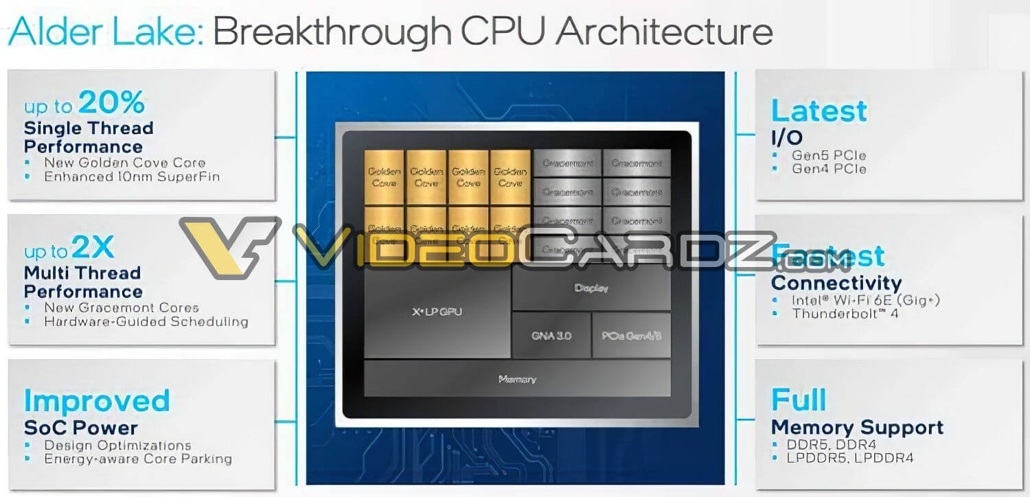
But in any case, according to the official slide Intel has highlighted the Alder Lake-S CPU lineup as a “Breakthrough CPU Architecture”. The company also claims that these new hybrid processors will offer a 20% single-threaded performance uplift and a 2X uplift in multi-threaded tasks.
The block diagram clearly mentions that Alder Lake will feature both high performance big cores, and high efficiency small cores on the die. The Golden Cove cores will serve as the big cores on the CPU & will feature simultaneous multi-threading support, while small Atom gracemont cores will stick to a non-SMT design.
Some new features for the cores themselves will include Hardware-Guided Scheduling, Design Optimizations, and Energy-aware core parking.
The block diagram slide confirms that the full chip is going to offer up to 8 Golden Cove big cores, and up to 8 Gracemont small cores. But again, previous leaks and rumors have already given us hint about this hybrid CPU architecture.
It is confirmed that Alder Lake will support PCI Express Gen5 and Gen4. There is also a confirmation on DDR5 and DDR4 memory support. The platform will support both these memory types.
We have some details on the new Intel “600 series chipset” motherboard lineup as well. Alder Lake CPU platform will support a brand new 600-series platform, and the Z690 chipset will be the flagship high-end motherboard model.
It has been mentioned that the premium Z690 motherboards will be able to support dual-channel DDR5 memory with native speeds of up to 4800 MHz, whereas cheaper budget-tier chipsets (e.g. the H670, B650, H610) will offer DDR4-3200 support.
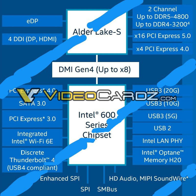
Lastly, the Intel Alder Lake CPUs will feature 16 PCIe Gen 5.0 and 4 PCIe Gen 4.0 lanes. The chipset itself will also support Gen 4 and Gen3. Direct Media Interface (DMI) has also been upgraded to Gen 4.
Alder Lake processors have already been confirmed before to support a new LGA 1700 socket.
As the name implies, the LGA1700 socket is comprised of 1,700 pins, which gives us 500 more pins that the existing LGA1200 socket that houses Comet Lake-S and the upcoming Rocket Lake-S series of processors. The upcoming LGA1700 socket board will have support for three generations of CPUs.
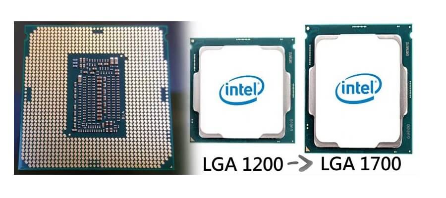
The socket dimensions for LGA1700 are 37.5mm x 45mm, which is about 7.5mm taller than Intel’s current LGA1200 socket. The bigger size is to house larger core counts than the Rocket Lake-S lineup which are currently planned for release on March 30, 2021.
From the picture we can see the Alder Lake CPU having a more rectangular shape, a new larger form factor, whereas the LGA1200 socket is square shaped. So Alder lake processors won’t be compatible with existing motherboard chipsets, as they will require a new socket LGA1700 motherboard.
The land grid array pin layout remains the same as evident from the die picture, and there are a total of 1700 gold contact pads as well.
As I said before, Alder Lake CPU lineup will bring the concept of heterogeneous multi-core to x86 processors for client PCs. High-end Alder Lake CPUs are expected to have up to 16 cores. The next-gen Alder Lake-S CPUs will use a new Hybrid Core/Atom processor architecture.
“Just to recap some of the previous findings/leaks on Alder Lake platform specs. But make a note that the following technical info on Alder Lake CPU lineup has not been officially confirmed by Intel yet. So exercise some caution here.”
Back in July 2020, a new GNU compiler update was posted by Phoronix, which included a list of compatible instructions for both Intel’s upcoming data center/HPC Sapphire Rapids chips and the Alder Lake desktop chips. According to the GNU update Alder Lake-S CPU lineup was noticeably missing full support for the AVX-512, a SIMD instruction recently introduced by Intel for its desktop chips.
These instruction sets are also disabled in Intel’s latest hybrid Lakefield chips.
This is done to keep the instruction set more consistent between cores (small Atom Tremont cores lack support for AVX instructions though). This also eases the operating system scheduling routines that target different workloads at the corresponding cores.
Therefore, the lack of AVX-512 support for Alder Lake-S serves as further evidence that Intel will bring a new hybrid core architecture design to desktop PCs.
However, it should be noted that while the lack of AVX-512 support hints at a hybrid design, the Alder Lake ‘support matrix’ has a listing of standard AVX instructions that are not supported by the current generation Atom Tremont cores.
So this means that the next generation of Atom Gracemont cores, which are largely considered ‘small’ cores used in Alder Lake, could bring AVX support, albeit in a limited manner.
The Sapphire Rapids chips on the other hand support many AVX instructions, like for example AVX512F, CLWB, AVX512VL, AVX512BW, AVX512DQ, AVX512CD, AVX512VNNI, and the new AVX512BF16 that enables support for bfloat 16, which is a compact numerical format having similar performance to FP32, but with only half the bits.
The Alder Lake-S CPU architecture will also feature the CLDEMOTE ‘cache line demote instruction’ set, which I’ve explained in this article.
Though, to reiterate, the CLDEMOTE instruction hints to hardware that the cache line that contains the linear address should be moved (demoted) from the cache(s) closest to the processor core to a level more distant from the processor core.
CLDEMOTE instructions are used so that the OS can tell the processor core which specific line in the cache is no longer needed, and its contents can be moved elsewhere, however, not directly into the main operating memory, but still into the processor cache, at higher levels (from L1 to L2 and from L2 to L3).
Also, according to one report posted by Zhihu, the new hybrid technology in the upcoming Alder Lake architecture would allow both CPU cores (small and big) to share the same instruction set and registers, but the actual availability of certain instructions would depend on which core is actually enabled and active.
The user also shared a screenshot from Intel’s internal document which suggests that the following AVX-512, TSX-NI, and the FP16 instruction sets will be disabled when the Hybrid Technology is enabled (both Big and Small cores are enabled at the same time).
The instructions will only work when the hybrid technology is disabled, which means the small cores are disabled. By disabled we can think of the processor’s mode/PL state, though I need more technical info to confirm how this will work on desktop PCs.
Both the big and small cores will have the same amount of instruction sets and model-specific registers, but will have different computational powers, and the overhead will also differ.
We can assume the big cores to have higher throughput and clock speeds, whereas the small cores are going to be more power efficient. So the following instruction sets, e.g. AVX512, Intel TSX and FP16, are only going to work on the BIG cores.
ARM’s Big/Small core architecture makes more sense for mobile devices, to conserve power, but we still don’t know how this Hybrid technology is going to actually work on Desktops.
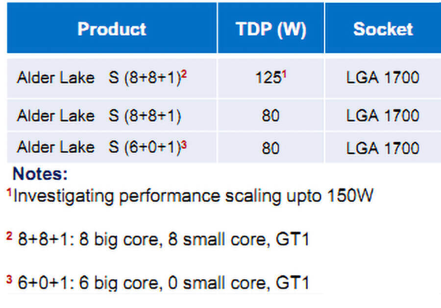
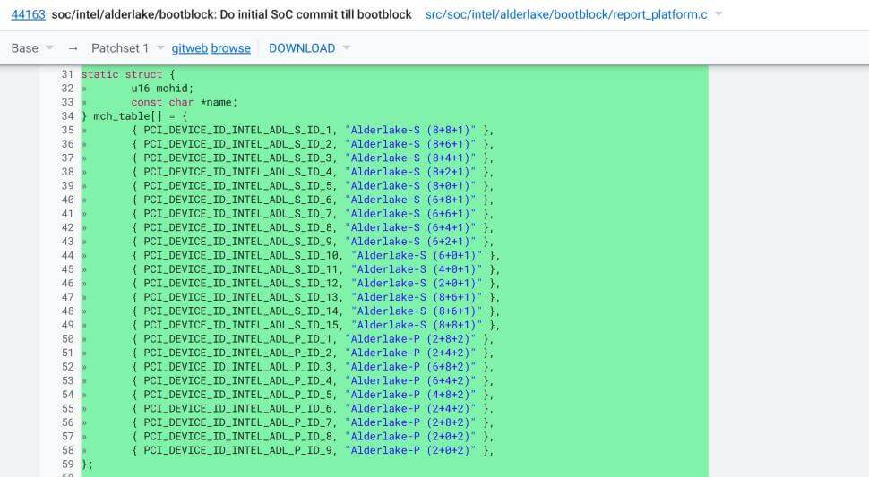
As per one coreboot leaked code spotted back in August 2020, the full configuration of the Alder Lake series of CPUs, namely the CPU, GPU and the PCH was also detailed to some extent. It appears we would be getting several Alder Lake CPU variants, in the Alder Lake S and P-Series configurations. This can get a bit confusing though because of the “segmentation”.
For example, the reported config numbers ‘8+8+1’ actually refer to the BIG, SMALL, and GPU core counts respectively. So we assume all variants will indeed have the small cores on desktop as well. So expect a maximum of 2 to 8 big cores, and up to 0 to 8 small cores.
These are some internal codenames for the Platform Controller Hub (PCH). It seems that Intel will use four PCHs with distinct features to cater to different market segments. These appear to be the Base, Mainstream, Premium and the Super Tier platforms.
- { PCI_DEVICE_ID_INTEL_ADP_P_ESPI_0, “Alderlake-P-Base SKU” },
- { PCI_DEVICE_ID_INTEL_ADP_P_ESPI_1, “Alderlake-P-Super SKU” },
- { PCI_DEVICE_ID_INTEL_ADP_P_ESPI_2, “Alderlake-P Premium SKU” },
- { PCI_DEVICE_ID_INTEL_ADP_P_ESPI_3, “Alderlake-P Mainstream SKU” },
- { PCI_DEVICE_ID_INTEL_ADP_P_ESPI_4, “Alderlake-P-Base SKU” },
- { PCI_DEVICE_ID_INTEL_ADP_P_ESPI_5, “Alderlake-P-Base SKU” },
- { PCI_DEVICE_ID_INTEL_ADP_P_ESPI_6, “Alderlake-P Super SKU” },
- { PCI_DEVICE_ID_INTEL_ADP_P_ESPI_7, “Alderlake-P Premium SKU” },
- { PCI_DEVICE_ID_INTEL_ADP_P_ESPI_8, “Alderlake-P-Base SKU” },
- […]
- { PCI_DEVICE_ID_INTEL_ADP_S_ESPI_0, “Alderlake-S-Base SKU” },
- { PCI_DEVICE_ID_INTEL_ADP_S_ESPI_1, “Alderlake-S-Super SKU” },
- { PCI_DEVICE_ID_INTEL_ADP_S_ESPI_2, “Alderlake-S Premium SKU” },
- { PCI_DEVICE_ID_INTEL_ADP_S_ESPI_3, “Alderlake-S Mainstream SKU” },
- { PCI_DEVICE_ID_INTEL_ADP_S_ESPI_4, “Alderlake-S-Base SKU” },
- { PCI_DEVICE_ID_INTEL_ADP_S_ESPI_5, “Alderlake-S-Base SKU” },
- { PCI_DEVICE_ID_INTEL_ADP_S_ESPI_6, “Alderlake-S Super SKU” },
- { PCI_DEVICE_ID_INTEL_ADP_S_ESPI_7, “Alderlake-S Premium SKU” },
- { PCI_DEVICE_ID_INTEL_ADP_S_ESPI_8, “Alderlake-S-Base SKU” }
Intel has not announced any exact launch date for Alder Lake-S processors yet, but since Alder Lake-S is the successor to Tiger Lake and Rocket Lake, so these new hybrid core processors will debut by the end of this year, 2021.
Stay tuned for more tech news!
Hello, my name is NICK Richardson. I’m an avid PC and tech fan since the good old days of RIVA TNT2, and 3DFX interactive “Voodoo” gaming cards. I love playing mostly First-person shooters, and I’m a die-hard fan of this FPS genre, since the good ‘old Doom and Wolfenstein days.
MUSIC has always been my passion/roots, but I started gaming “casually” when I was young on Nvidia’s GeForce3 series of cards. I’m by no means an avid or a hardcore gamer though, but I just love stuff related to the PC, Games, and technology in general. I’ve been involved with many indie Metal bands worldwide, and have helped them promote their albums in record labels. I’m a very broad-minded down to earth guy. MUSIC is my inner expression, and soul.
Contact: Email