
Intel’s next generation of Alder Lake-S Core processors are said to be the company’s first 10nm-based mainstream desktop processors, and we have already seen documents, datasheets, and release notes for these CPUs which also appeared on Intel’s own developer website. These processors have been confirmed to support a new LGA 1700 socket as well.
— 188号 (@momomo_us) June 26, 2020
Back in July, Intel confirmed that its next-gen 10nm Alder Lake-S CPU lineup will launch in the second half of 2021. Intel has also confirmed that the next-gen Alder Lake-S CPUs will use a new Hybrid Core/Atom processor architecture. These next-gen CPUs are expected to support the DDR5 memory and PCIe 4.0 or 5.0 interface. As the name implies, the LGA1700 socket is comprised of 1,700 pins, which gives us 500 more pins that the existing LGA1200 socket that houses Comet Lake-S and the upcoming Rocket Lake-S series of processors.
The upcoming LGA1700 socket board will have support for three generations of CPUs. This is something new for Intel because the company has been known to support a short socket lifespan till now. These findings indicate that Intel’s LGA1700 socket will compete with AMD’s AM5 socket in terms of platform longevity.
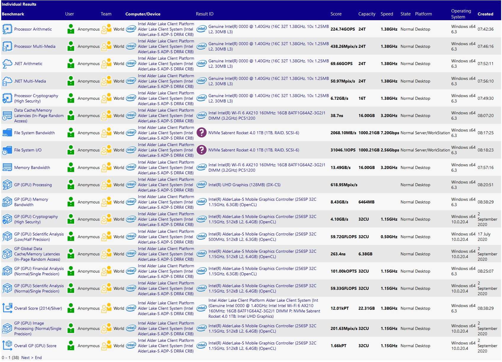
Now, renowned Hardware leaker @Tum_Apisak has recently spotted some SiSoftware benchmark submissions for one of Intel’s future Alder Lake-S processors.
Intel AlderLake-S ADP-S DRR4 CRB
Genuine Intel(R) 0000 @ 1.40GHz
(16C 32T 1.38GHz, 10x 1.25MB L2, 30MB L3)https://t.co/bNosaT4eNG pic.twitter.com/KgPOolRRQS— APISAK (@TUM_APISAK) October 6, 2020
The database has detected the CPU with having 16 physical cores and 32 threads, which could possibly mean the maximum core count for the Alder Lake-S lineup. Although a 16C/32T configuration has been spotted, but the software reports 16 cores and 24 threads, in some of the benchmarks. This means the SiSoftware’s benchmark might not be optimized for this hybrid chip. Therefore, you should take this Alder Lake-S CPU entry with a grain of salt. This would be an actual 8 physical cores processor though, since it is based on a new Hybrid big+small core design and architecture.
The CPU is detected having 10x 1.25MB of L2 cache and 30MB of L3 cache. SiSoftware lists the Alder Lake-S processor with a clock speed of 1.4 GHz (possibly for the Gracemont cores). The iGPU comes equipped with 256 shader cores clocked at 1.15 GHz, which seems to correlate with the previous submission as well.
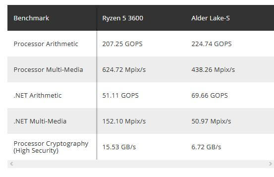
For what it’s worth, the Alder Lake-S seems to beat the Ryzen 5 3600 in the Processor Arithmetic and .NET Arithmetic benchmarks. Table/chart courtesy of Tom’s Hardware.
Alder Lake-S CPU lineup will be the first Intel architecture to offer ARM’s big.LITTLE approach to desktop processors. Alder Lake-S would feature an 8+8 core configuration, in which half the cores are going to be Big Cores and the rest of the remaining would be Small Cores. These processors would thus feature a total of 16 cores in a single package.
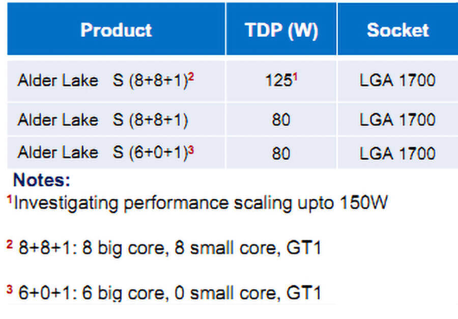
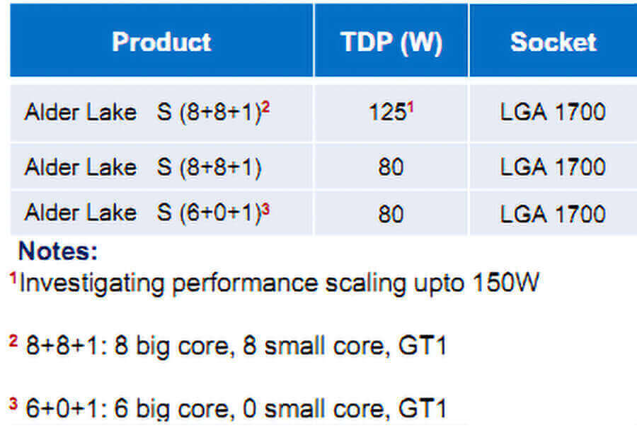
According to one report these architectures are Golden Cove (Willow Cove successor) and Gracemont (Tremont successor), respectively. Willow Cove is expected to appear in the upcoming Rocket Lake-S series of processors. Few months back, it was reported that Alder Lake-S processor will be available in three combinations. For example, the reported configuration numbers 8+8+1 actually refer to the BIG, SMALL, and GPU core counts, respectively.
Back in July, a new GNU compiler update was posted by Phoronix, which included a list of compatible instructions for both Intel’s upcoming data center/HPC Sapphire Rapids chips and the Alder Lake desktop chips, with Alder Lake noticeably missing full support for the AVX-512, a SIMD instruction recently introduced by Intel for its desktop chips.
These instruction sets are also disabled in Intel’s latest hybrid Lakefield chips. This is done to keep the instruction set more consistent between cores (small Atom Tremont cores lack support for AVX instructions though). This also eases the operating system scheduling routines that target different workloads at the corresponding cores. Therefore, the lack of AVX-512 support for Alder Lake-S serves as further evidence that Intel will bring a new hybrid core architecture design to desktop PCs.
However, it should be noted that while the lack of AVX-512 support hints at a hybrid design, the Alder Lake ‘support matrix’ has a listing of standard AVX instructions that are not supported by the current generation Atom Tremont cores. So this means that the next generation of Atom Gracemont cores, which are largely considered ‘small’ cores used in Alder Lake, could bring AVX support, albeit in a limited manner.
The Sapphire Rapids chips on the other hand support many AVX instructions, like for example AVX512F, CLWB, AVX512VL, AVX512BW, AVX512DQ, AVX512CD, AVX512VNNI, and the new AVX512BF16 that enables support for bfloat 16, which is a compact numerical format having similar performance to FP32, but with only half the bits.
The Alder Lake-S CPU architecture will also feature the CLDEMOTE ‘cache line demote instruction’ set, which I’ve explained in details in my previous article. Though, to reiterate, the CLDEMOTE instruction hints to hardware that the cache line that contains the linear address should be moved (demoted) from the cache(s) closest to the processor core to a level more distant from the processor core.
CLDEMOTE instructions are used so that the OS can tell the processor core which specific line in the cache is no longer needed, and its contents can be moved elsewhere, however, not directly into the main operating memory, but still into the processor cache, at higher levels (from L1 to L2 and from L2 to L3).
Also, according to one recent report posted by Zhihu, the new hybrid Technology in the upcoming Alder Lake architecture would allow both CPU cores (small and big) to share the same instruction set and registers, but the actual availability of certain instructions would depend on which core is actually enabled and active. The user also shared a screenshot from Intel’s internal document which suggests that the following AVX-512, TSX-NI, and the FP16 instruction sets will be disabled when the Hybrid Technology is enabled (both Big and Small cores are enabled at the same time).
The instructions will only work when the hybrid technology is disabled, which means the Small cores are disabled. By disabled we can think of the processor’s mode/PL state, though I need more technical info to confirm how this will work on Desktop PCs. Both the big and small cores will have the same amount of instruction sets and model-specific registers, but will have different computational powers, and the overhead will also differ.
We can assume the big cores to have higher throughput and clock speeds, whereas the small cores are going to be more power efficient. Like mentioned before, the following instruction sets, e.g. AVX512, Intel TSX and FP16, are only going to work on the Big cores. The ARM’s Big/Small core architecture makes more sense for mobile devices, to conserve power, but we still don’t know how this Hybrid technology is going to actually work on Desktops.
Intel has not announced any exact launch date for Alder Lake-S processors yet, but since the Alder Lake-S is the successor to Tiger Lake, so the processors will debut as the 12th Generation Core lineup next year, second half of 2021.
On some other related news on INTEL processors, Videocardz reports that the upcoming Rocket Lake-S CPU lineup is now expected to launch around March 2021. This is a rumor so please exercise some caution here. While there have been rumors of Rocket Lake previously targeting CES 2021 as the launch window, it now seems that week 10 of 2021, i.e. March could be the actual launch date.
Rocket Lake (RKL) is a planned microarchitecture designed by Intel as a direct successor to the Comet Lake-S series of desktop CPUs and high-performance mobile devices. Intel has been using the same iteration of the 14nm FinFET process node with the Skylake Architecture for many years. Comet Lake-S was also fabbed on this aging process node, which has held Intel back in terms of IPC uplift and efficiency gains over AMD’s Ryzen lineup.
Rocket Lake-S desktop platform is going to be the last CPU architecture to be based on an advanced 14nm process node. Intel’s Rocket Lake will use a 14++ nm back-port of the Willow Cove core architecture. Rocket Lake is going to be the desktop equivalent of Tiger Lake. Rocket Lake-S will be housed on 500-series motherboards. A 500-series motherboard roadmap has also been leaked by HDTecnologia.
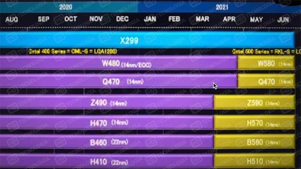
The above roadmap confirms that both the CPU and the new motherboard lineup will launch in March 2021. Although the Rocket Lake-S lineup will be the last to feature the LGA1200 socket, Intel is planning a full range of chipsets, including workstation W580, high-end gaming Z590, H570 and budget-oriented B560 and H510 series. According to the roadmap, the gaming 500 series is due to launch in late March.
The Rocket Lake CPU series will feature Intel’s Xe-based Gen12 integrated graphics, offering twice the performance over Gen 9.5 graphics.
According to previous rumors Rocket Lake will deliver desktop users up to eight cores and sixteen threads on the high-end, which means two cores and four threads less than the current Comet Lake processor lineup. But the reduction in core count could also mean that Intel plans to rely on increased single-threaded performance, thus boosting overall system performance through single-threaded gains.
Single-threaded performance will help Intel to compete more in the CPU market segment, even if AMD can deliver higher core count SKUs. Not all applications or tasks are highly multi-threaded in nature, which makes the single-threaded performance all the more important.
Few months ago one VLSI engineer who goes by the name @Retired Engineer on Twitter, @chiakokhua, tweeted one of his old findings from November 2019 last year. According to him the upcoming Rocket Lake-S processors are going to feature ‘multi-chip modules/MCM’ of core and uncore GPU dies built on different silicon fabrication nodes. This is speculation from his side, but he has a strong record of accurate prediction in the past, when he spoke about the 3rd gen Ryzen Matisse AM4 processors being multi-chip modules as well.
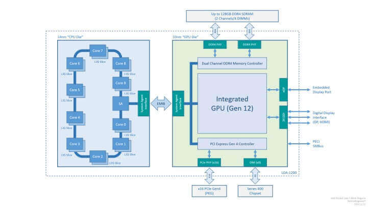
Apparently, it might be possible that Intel is also designing these socket LGA1200-based Rocket Lake processors to feature multi-chip modules, similar to Matisse in some way. According to the block diagram posted by @chiakokhua, we can see that the Rocket Lake-S architecture is a multi-chip module/MCM consisting of a 14nm die that holds the ‘CPU cores’; and a 10 nm die that holds the ‘uncore’ components.
But in the case of Rocket Lake the uncore die is more advanced that the CPU die. The CPU die is fabbed on a 14 nm node on Rocket Lake-S, which contains the Willow Cove CPU cores in this die, and a system agent, which are connected together by a Ring-bus interconnect. And the system agent connects to the 10nm uncore GPU die via EMIB.
The 10 nm GPU uncore die on the other hand features the Gen12 XE iGPU with up to 96 EUs, a dual-channel DDR4 memory controller, a PCI-Express 4.0 controller, as well as display and media engines. Rocket Lake-S MCM provides a total of 24 PCI-Express lanes, out of which 16 are assigned as PEG (PCI-Express Graphics), and 8 lanes are assigned as chipset bus. Comet Lake-S CPU lineup only provided us with 20 lanes.
This is not the first time Intel is taking the MCM approach. Clarkdale, first-gen desktop processor supporting the LGA1156 package was an MCM having a 32 nm CPU die, and a 45 nm uncore graphics and integrated memory controller die. It remains to be seen whether Intel really chooses the MCM approach with the Rocket Lake- S lineup of desktop processors.
Rocket lake-S CPUs are going to support the PCIe 4.0 standard and interface. The 11’th gen Rocket Lake-S desktop CPUs are also going to be compatible with the Z490 chipset and LGA 1200 socket motherboards. But this places Intel’s Z490 platform longevity in a difficult position, since the company won’t be supporting the LGA 1200 socket for long. The current Z490 chipset is only expected to support Comet Lake-S and Rocket Lake-S CPU series, since Alder Lake-S is already rumored to feature a new LGA1700 socket.
Speaking of next-gen Intel processors and platform, GIGABYTE confirmed that their Z490 AORUS lineup of motherboards are going to support limited PCI-E 4.0 capabilities on Comet Lake, which seems obvious since the Intel’s 10th generation Comet Lake-S series of processors do not fully support this new PCIe 4.0 standard. Since hardware-level support for PCIe 4.0 is already built-in these Z490 boards, only Rocket Lake CPUs are going to offer full compatibility of the PCIe Gen 4.0 standard.
PCIe 4.0 has been an AMD-only feature within the consumer market till now, but things might change with the launch of Rocket lake-S CPUs. For GAMING perspective, both Alder Lake and Rocket Lake CPUs are relevant for gamers looking to upgrade their systems.
Stay tuned for more!
UPDATE:
Intel has confirmed that its Rocket Lake-S CPUs will release in Q1 2021.
“Though as you’d expect, we’re constantly looking ahead at what’s next and how we can make our desktop CPUs even better. With that said, I’m also happy to confirm that the next generation 11th Gen Intel Core desktop processors (codenamed “Rocket Lake”) is coming in the first quarter of 2021 and will provide support for PCIe 4.0. It’ll be another fantastic processor for gaming, and we’re excited to disclose more details in the near future. There’s a lot more to come, so stay tuned!”
Hello, my name is NICK Richardson. I’m an avid PC and tech fan since the good old days of RIVA TNT2, and 3DFX interactive “Voodoo” gaming cards. I love playing mostly First-person shooters, and I’m a die-hard fan of this FPS genre, since the good ‘old Doom and Wolfenstein days.
MUSIC has always been my passion/roots, but I started gaming “casually” when I was young on Nvidia’s GeForce3 series of cards. I’m by no means an avid or a hardcore gamer though, but I just love stuff related to the PC, Games, and technology in general. I’ve been involved with many indie Metal bands worldwide, and have helped them promote their albums in record labels. I’m a very broad-minded down to earth guy. MUSIC is my inner expression, and soul.
Contact: Email