

Last month Intel’s senior Vice President, Raja Koduri, posted a teaser of the company’s first gaming discrete graphics cards on Twitter, the Xe HPG. Intel’s Xe HPG DG2 (High-Performance) gaming graphics card was tested in the new 3DMark Mesh Shader feature test.
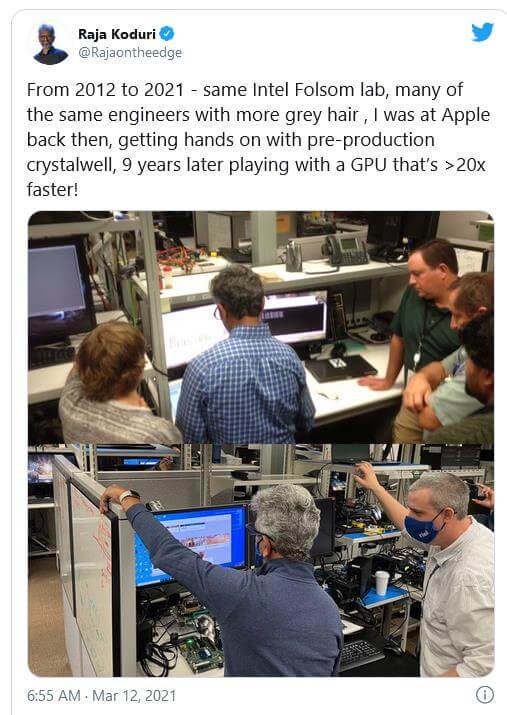
It now looks like he is teasing the same GPU once again. Raja Koduri recently posted a picture on his Twitter account from the Folsom, California lab at Intel, showcasing the new Xe-HPG graphics card which is being tested in some 3DMark benchmarks. We are talking about DXR or ray traced 3D test here.
Judging from the photo, this appears to be an engineering board with a large CPU-like heatsink and cooler attached to it, which implies that this should be the DG2 gaming graphics card in action.
Even though his Twitter account hasn’t mentioned anything about the GPU being tested, but if you look closely at the photo after enhancing/sharpening it, the 3DMark software that is installed on this test system in the lab has the entire 3DMark feature tests installed, including the DirectX DXR test.
The current Xe GPUs (based on the Xe-LP architecture) don’t support ray tracing, so this gives us a clue that the GPU being tested here could be the Xe-HPG “DG2” gaming graphics card. But of course this is all speculation for now.
But the 3DMark screen clearly shows the DXR test on the extreme right side of the window implying this is the Xe HPG (DG2) GPU.
The benchmark was running the test that could only have been run on the HPG GPU, and not Xe-LP. You can see the CPU-looking device with its own heat sink and cooler connected to a PCIe riser and cable and then into a motherboard.
We can also see two power supplies, one directly attached to the GPU board, while the other one is supplying power to the motherboard.


If Raja is teasing the DG2 gaming GPU then we are likely looking at on-shelve availability in a few months or so, hopefully.
“From 2012 to 2021 – same Intel Folsom lab, many of the same engineers with more grey hair , I was at Apple back then, getting hands on with pre-production crystalwell, 9 years later playing with a GPU that’s >20x faster!” –Raja Koduri.
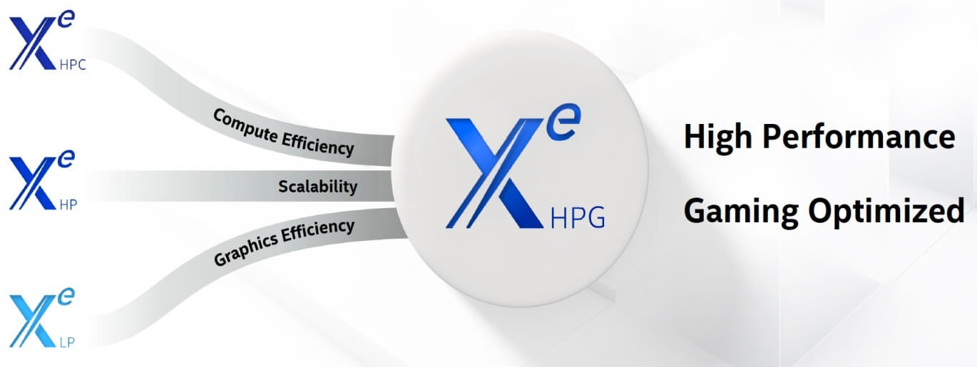
The Intel DG2 graphics appears to be the first GPU based on the HPG architecture. This graphics processor is rumored to offer up to 512 Execution Units, which gives the GPU 4096 cores (Shading Units). The card is based on the Gen12 graphics architecture.
The card will sport features like compute efficiency, scalability and graphics efficiency. Intel has also confirmed that the new HPG architecture will use the GDDR6 memory type.
Back in October 2020, Intel taped out its first discrete gaming GPU, the Xe-HPG ‘DG2’ graphics processor. The company reaffirmed back then that it is working on a full stack of discrete Xe-HPG-based GPUs that will target the mid-range/mainstream, and also the enthusiast gaming market segment sometime later this year.
The new Intel DG1 on the other hand, is Intel’s first discrete GPU in over 20 years. Intel’s DG1 GPU is already shipping in volume. DG1 is codenamed as Intel Iris Xe MAX GPU, which is used in ultraportable and thin laptop designs. It is based on the Xe-LP architecture for iGPUs and low-power models, and entry-level gaming PCs.
The new Intel DG2 discrete gaming graphics processor on the other hand was in “alpha silicon” form back then, but Intel said they’ve already powered-on this new DG2-based GPU in their labs. DG2 isn’t just a successor to DG1, but instead is a higher performing bracket GPU based on the company’s latest Xe-HPG architecture.
Xe-HPG is the enthusiast, and gaming-focused GPU architecture, incorporating hardware-enabled features found in similar discrete GPUs from AMD and NVIDIA like e.g. ray tracing/RTX etc.
Intel’s family of Xe-HPG graphics processors will consist of multiple SKUs targeting different market segments spanning all the way from mid-range to the high-end enthusiast level.
This GPU was already rumored to be manufactured outside of Intel’s fab, in an external foundry. Back then while Intel didn’t mention which fab and process node was going to be used, but as per one report from REUTERS, they might tap TSMC’s enhanced 7nm process node, or maybe even 6nm node.
Intel has actually used a lot of other third-party IP, such as the memory controller and interface, and display interface to optimize the overall design costs.
Though, Intel hasn’t clarified whether DG2 is a flagship-grade bigger chip, or a more modest, and smaller high-volume part. For now, the company is simply saying that DG2 will, “take our discrete graphics capability up the stack into the enthusiast segment.”
Recently, some leaked specs of Intel’s upcoming XE-HPG (High-Performance gaming) “DG2” GPU lineup were shared by twitter user @harukaze5719. More details can be found in this article.

Intel is expected to unveil its DG2-based graphics cards later this year. Though at the recent January 11 CES 2021 event, there was no mention of this discrete gaming GPU.
Stay tuned for more tech news!
UPDATE:
It appears that Intel’s DG2 (Xe-HPG) discrete GPU has just been spotted alongside a 16-core Alder Lake-S CPU, within the Geekbench database with some specifications. Coming via @TUM_APISAK.
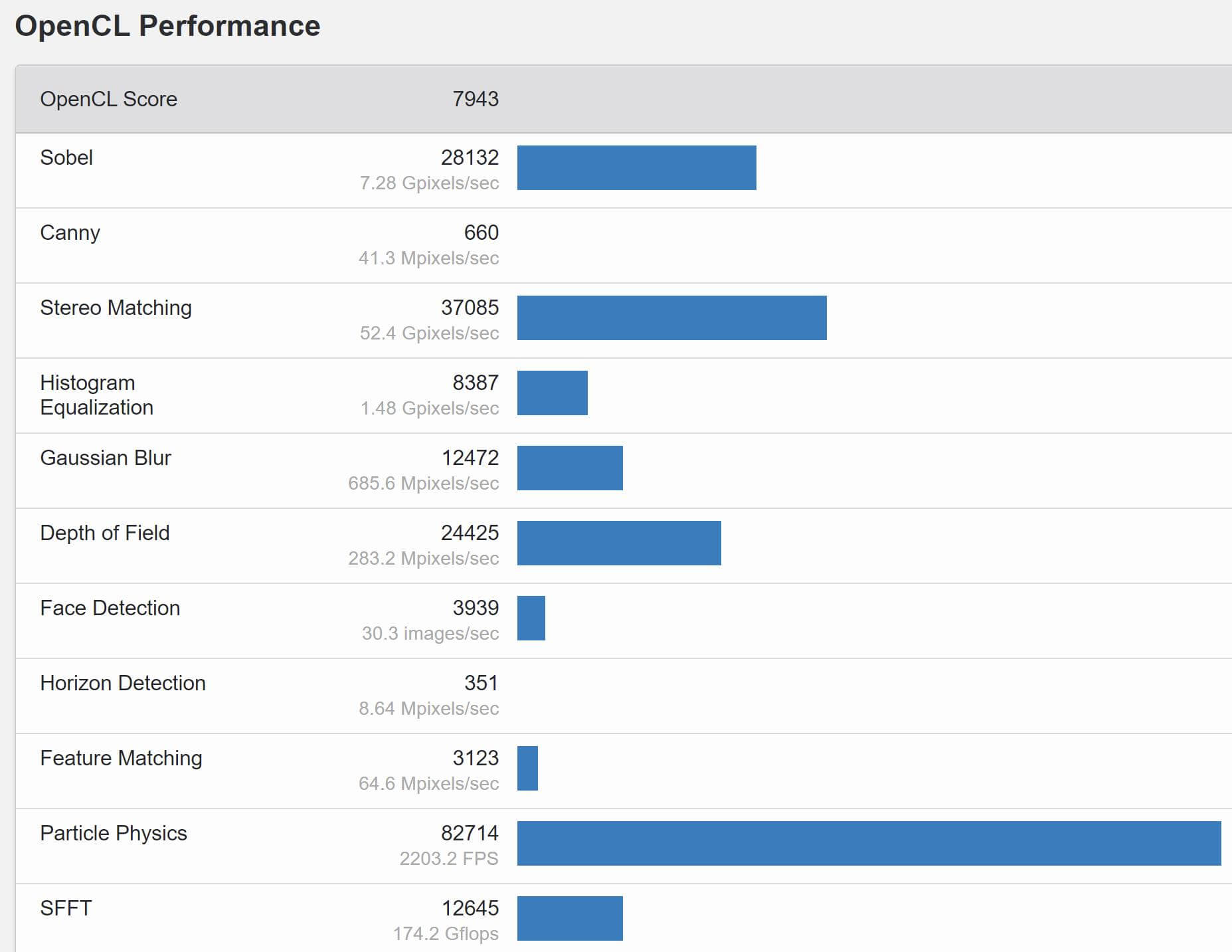
The Intel Xe-HPG DG2 GPU spotted features 512 Execution units which amounts to 4096 cores. The GPU clock speed has been listed as 1800 MHz (max), though we don’t know if this will be the final clock speed since the GPU tested here could also be an early engineering sample/ES.
The card is listed with a 12.6 GB memory capacity/VRAM but this seems inaccurate since the benchmark is unable to properly identify the VRAM capacity. The most interesting part is that this Xe-HPG DG2 GPU was tested on an Intel Alder Lake-S Desktop CPU platform, socket 1700 LGA.
The platform features a 12th gen core processor having 16 cores and 24 threads. The CPU is clocked at 2.20 GHz for the base clock and 4.60 GHz for the boost, Though, we don’t know whether the base and boost frequencies listed here are for the high-efficiency (small) cores or the high-performance (big) cores.
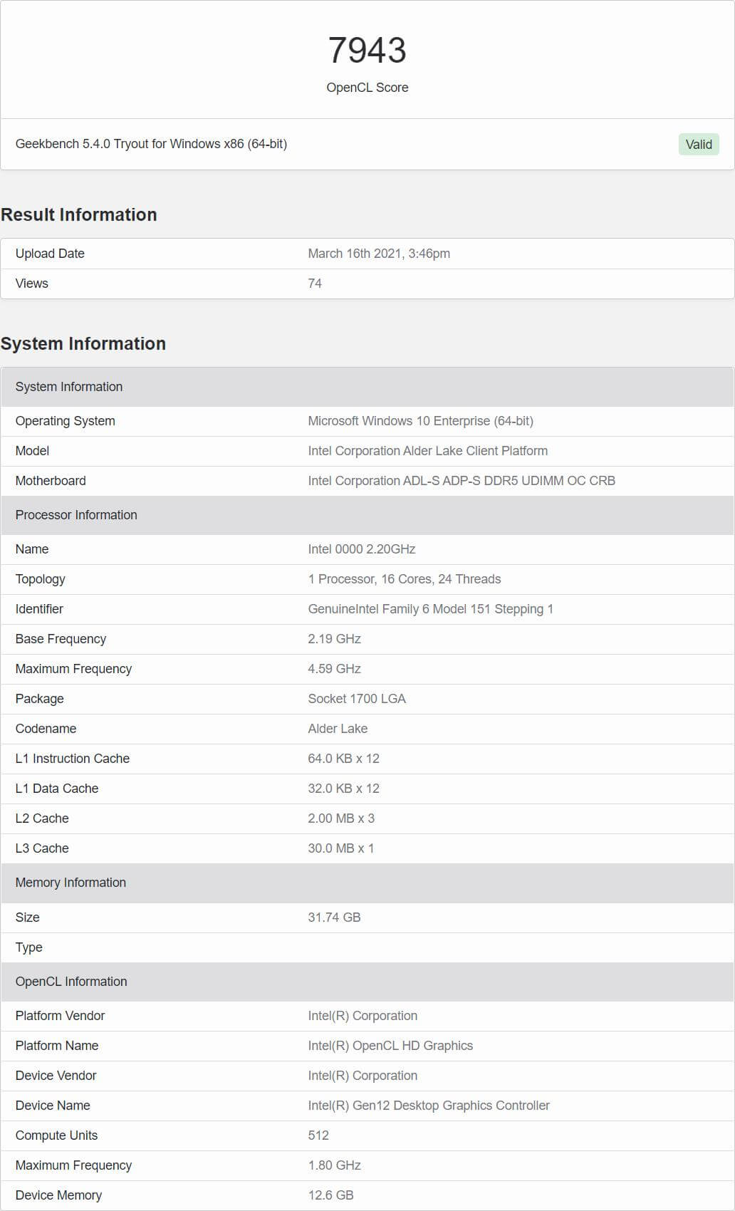
Since the GPU is not running at its full potential, the OpenCL (GPU) result is really bad, even worse than the GeForce 500 series GPUs based on the Fermi architecture. This could also be due to a driver issue which might not be fully optimized.
Hello, my name is NICK Richardson. I’m an avid PC and tech fan since the good old days of RIVA TNT2, and 3DFX interactive “Voodoo” gaming cards. I love playing mostly First-person shooters, and I’m a die-hard fan of this FPS genre, since the good ‘old Doom and Wolfenstein days.
MUSIC has always been my passion/roots, but I started gaming “casually” when I was young on Nvidia’s GeForce3 series of cards. I’m by no means an avid or a hardcore gamer though, but I just love stuff related to the PC, Games, and technology in general. I’ve been involved with many indie Metal bands worldwide, and have helped them promote their albums in record labels. I’m a very broad-minded down to earth guy. MUSIC is my inner expression, and soul.
Contact: Email