
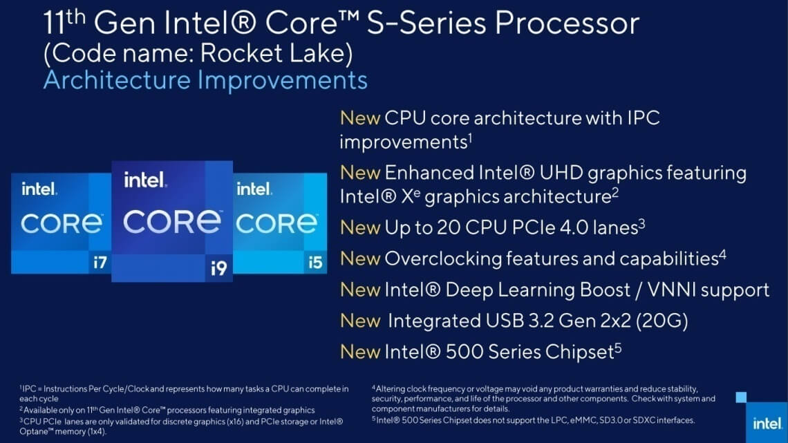
Last month, Intel officially revealed its upcoming 11th Gen Rocket Lake-S desktop CPU lineup, based on the Cypress Cove core architecture. Rocket Lake (RKL) is a planned microarchitecture designed by Intel as a direct successor to the Comet Lake-S series of desktop CPUs and high-performance mobile devices.
RKL processor family will release in the first quarter of 2021, and is expected to share the same socket and motherboard compatibility as the current 10th Gen Comet Lake processors, thus providing an upgrade path even for those rocking the flagship Core i9-10900K Comet lake CPU.
Rocket Lake-S desktop platform should hopefully be the last CPU architecture to be based on an advanced 14nm process node. The new Rocket Lake-S silicon or SoC is going to be known as ‘Cypress Cove’.
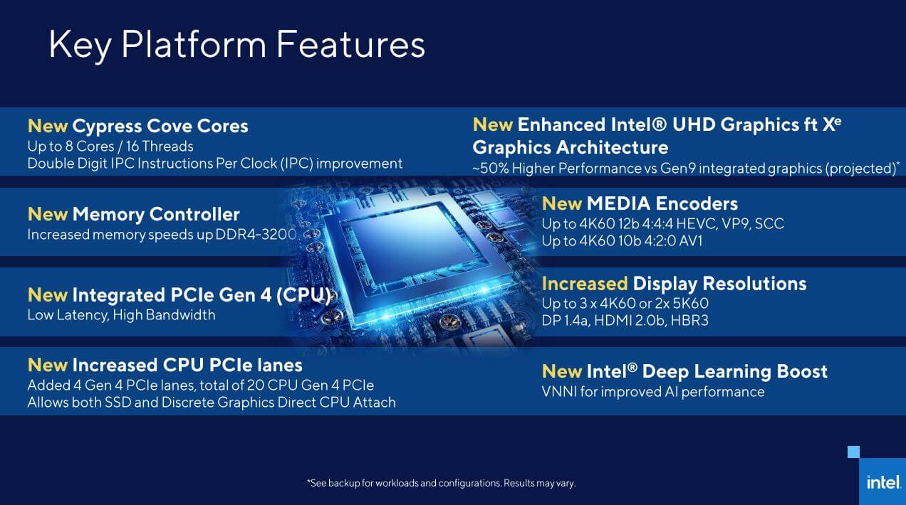
Rocket Lake-S will offer PCIe Gen 4.0 support, enhanced overclocking and double-digit percentage IPC benefits over Comet Lake-S lineup. Intel’s Rocket Lake will use a 14nm back-port of the 10nm Sunny Cove cores found in the Ice Lake processors. With Rocket Lake processors, Intel is targeting a raw instruction-per-clock uplift in the double digit range.
A recent single-threaded Cinebench R20 score posted by CapFrameX seems to hint that Intel plans to retake the lead in gaming performance with its future Rocket Lake processors, or at least close the gap even more. But to achieve this score the CPU was running at a massive 5.5 GHz boost clock.
🚀Rocket Lake🚀
CB 20 ST score
Rocket Lake 655
R9 5950X 649— CapFrameX (@CapFrameX) November 12, 2020
The Rocket Lake CPU sample scored 655 points in Cinebench R20, which makes it marginally ahead than the AMD Ryzen 9 5950X CPU which scores 649 points. The AMD Radeon R9 5950X has a maximum boost clock of 4.9 GHz, though the processor can cross over 5 GHz+ in some real-world benchmarks and testing.
Even though Cinebench is not a benchmark to judge the actual performance in games, its single-core scores are still interesting to check per-core CPU performance, and also because not many games benefit and scale from a multi-core chip (depends on the game though). So at least we can draw a parallel conclusion to some extent.
But nonetheless, the single-threaded Cinebench R20 result/score of this RKL CPU sample does look promising.
For what it’s worth, Intel’s 10-core i9-10900K CPU is still very competitive in games as compared to 12 and 16-core AMD Ryzen processors. So does this mean INTEL’s future processor lineup will surely take the Gaming performance crown from AMD ? Not necessary.
I guess only time will tell, since we need actual third-party gaming benchmarks to come to any conclusion. And there is also one catch.
To achieve a massive 5.5 GHz boost clock, the power consumption is going to be enormous, and it will also require some serious cooling as well, which is not what an average gamer prefers to do. This is also one of the main reasons the RKL CPU lineup will max out at 8 cores/16 threads. This is all because of the backporting the large CPU cores originally designed for 10nm to the older legacy 14nm node.
According to Intel, Rocket Lake-S will have a PL1 state value of 125 W and a PL2 of 250 W. Intel has also bumped the memory clock speeds up to DDR4-3200, an increase over the current DDR4-2933 speed supported on Comet Lake processors.
RKL lineup will also feature enhanced Intel UHD graphics that will use the company’s new Xe GPU architecture, which is projected to provide a 50 percent performance gain over Intel’s Gen9 graphics used on ninth-generation Intel Core processors.
“Rocket Lake processors will deliver amazing performance and flexibility to meet a range of needs for gamers and content creators,” -Intel.
Other new features include first-time support for PCIe Gen 4.0 in an Intel desktop processor; with up to 20 lanes that can support direct CPU attach for both SSDs and discrete graphics cards. Rocket Lake will also come with new media encoders for 4K, 60-frames-per-second video; increased display support for up to three 4k monitors or two 5K monitors.
Along with features like Intel Deep Learning Boost, VNNI (Vector Neural Network Instructions), Quick Sync Video, and better overclocking tuning. The platform will also integrate USB 3.2 Gen2x2 with speeds up to 20Gbps.
Intel’s Xe graphics introduces support for high end video decoders like 4:4:4 HEVC and VP9 while allowing display resolutions of up to 3x 4k60, or two 5K60 displays, also supporting DP 1.4a (with HBR3) and HDMI 2.0b.
New media encoders and display resolution support, with up to 4K60 12-bit for 4:4:4 HEVC and VP9, or up to 4K60 with 10-bit 4:2:0 AV1.
With Rocket Lake processors, Intel is targeting a raw instruction-per-clock uplift in the double digit range. My guess is that it would be at least 10%+. One of the main advantages of moving to a back-ported Sunny Cove core has been the inclusion of the AVX-512 vector acceleration unit in Cypress Cove.
This enables a library of Deep Learning Boost technologies for AI and ML acceleration, including support for the Vector Neural Network Instructions (VNNI), thus bringing AVX-512 support to the desktop platform.
Rocket Lake-S will be housed on the 500-series motherboards. Although the Rocket Lake-S lineup will be the last to feature the LGA1200 socket/Z490 chipset, Intel is planning a full range of chipsets, including workstation W580, high-end gaming Z590, H570, and budget-oriented B560 and H510 series.
According to one recent roadmap, the gaming 500 mobo series is due to launch in late March, next year 2021. Intel has also broadened the DMI interface, which connects the processor to the platform controller hub (PCH), from x4 to x8.
John Bonini (VP and GM of Client Computing Group Desktop, Workstation, and Gaming at Intel) has also confirmed that the 11th Gen Core series processors codenamed Rocket Lake will be Intel’s first lineup to support the PCI-Express gen 4.0 interface, a feature which has been seemingly missing in Intel’s client Desktop CPU platform for quite some time.
Rocket Lake will deliver desktop users up to eight cores and sixteen threads on the high-end, which means two cores and four threads less than the current Comet Lake processor lineup. But the reduction in core count could also mean that Intel plans to rely on increased single-threaded performance, thus boosting overall system performance through single-threaded gains.
Single-threaded performance will help Intel to compete more in the CPU market segment, even if AMD can deliver higher core count SKUs. Not all applications or tasks are highly multi-threaded in nature, which makes the single-threaded performance all the more important.
Few months ago one VLSI engineer who goes by the name @Retired Engineer on Twitter, @chiakokhua, tweeted one of his old findings from November 2019 last year. According to him the upcoming Rocket Lake-S processors are going to feature ‘multi-chip modules/MCM’ of core and uncore GPU dies built on different silicon fabrication nodes.This is speculation from his side, but he has a strong record of accurate prediction in the past, when he spoke about the 3rd gen Ryzen Matisse AM4 processors being multi-chip modules as well.
Apparently, it might be possible that Intel is also designing these socket LGA1200-based Rocket Lake processors to feature multi-chip modules, similar to Matisse in some way.
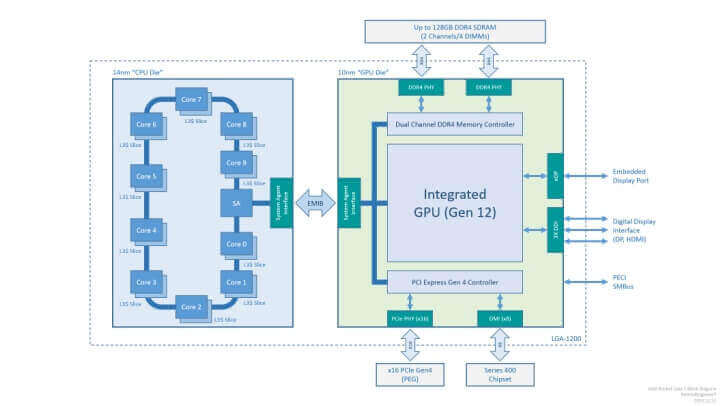
According to the block diagram posted by @chiakokhua, we can see that the Rocket Lake-S architecture is a multi-chip module/MCM consisting of a 14nm die that holds the ‘CPU cores’; and a 10 nm die that holds the ‘uncore’ components.
But in the case of Rocket Lake the uncore die is more advanced that the CPU die. The CPU die is fabbed on a 14 nm node on Rocket Lake-S, and a system agent, which are connected together by a Ring-bus interconnect. And the system agent connects to the 10nm uncore GPU die via EMIB.
The 10 nm GPU uncore die on the other hand features the Gen12 XE iGPU with up to 96 EUs, a dual-channel DDR4 memory controller, a PCI-Express 4.0 controller, as well as display and media engines. Rocket Lake-S MCM may provide a total of 20 or even 24 PCI-Express lanes, out of which 16 are assigned as PEG (PCI-Express Graphics), and 8 lanes are assigned as chipset bus.
You can see the Block diagram as posted below. This is not the first time Intel is taking the MCM approach. Clarkdale, first-gen desktop processor supporting the LGA1156 package was an MCM having a 32 nm CPU die, and a 45 nm uncore graphics and integrated memory controller die.
It remains to be seen whether Intel really chooses the MCM approach with the Rocket Lake- S lineup of desktop processors.
Stay tuned for more!
Hello, my name is NICK Richardson. I’m an avid PC and tech fan since the good old days of RIVA TNT2, and 3DFX interactive “Voodoo” gaming cards. I love playing mostly First-person shooters, and I’m a die-hard fan of this FPS genre, since the good ‘old Doom and Wolfenstein days.
MUSIC has always been my passion/roots, but I started gaming “casually” when I was young on Nvidia’s GeForce3 series of cards. I’m by no means an avid or a hardcore gamer though, but I just love stuff related to the PC, Games, and technology in general. I’ve been involved with many indie Metal bands worldwide, and have helped them promote their albums in record labels. I’m a very broad-minded down to earth guy. MUSIC is my inner expression, and soul.
Contact: Email