

In 2020’s second-quarter earnings press release, Intel confirmed that their next-gen Alder Lake-S CPU lineup will launch in late 2021. Intel also gave an update to analysts and investors on two crucial CPU projects of the company, namely 12th gen Alder Lake CPU lineup for the consumer desktop PC, and Sapphire Rapids chips for the HPC, and data centre/server market.
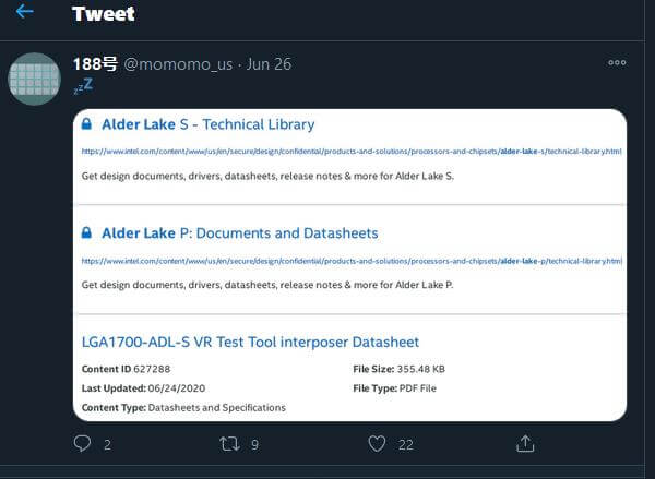
Alder Lake-S Hybrid x86 desktop processors are currently being sampled to customers as well. Intel’s 12th generation of Alder Lake-S Core processors are said to be the company’s first 10nm SuperFin-based mainstream desktop processors, and we have already seen documents, datasheets, and release notes for these CPUs which have also appeared on Intel’s own developer website.
The 10 nm Enhanced SuperFin process technology was originally designed for datacenter/HPC market segment and its products in mind, to provide enhancements to the power delivery system, MEOL and BEOL etc, in semiconductor terms.
Alder Lake CPU lineup will bring the concept of heterogeneous multi-core to x86 processors for client PCs. High-end Alder Lake CPUs are expected to have up to 16 cores. Alder Lake-S CPU lineup will be the first Intel architecture to offer ARM’s big.LITTLE approach to desktop processors.
Alder Lake-S would feature an 8+8 core configuration, in which half the cores are going to be BIG Cores and the rest of the remaining would be small Cores. These processors would thus feature a total of 16 cores in a single package, at least initially.
According to one report, these architectures are Golden Cove (Willow Cove successor) and Gracemont (Tremont successor), respectively. Willow Cove is expected to appear in the upcoming 11th gen Rocket Lake-S series of processors.
Recently one 16 cores, 24 threads Alder Lake-S early CPU sample has been spotted in the Geekbench database by TUM_APISAK. The clock speeds appear to be very low though, and the processor chip appears to be a part of the ‘GenuineIntel Family 6 Model 151 Stepping 0’ identifier.
This early engineering sample/ES appears with a base clock of just 1.38 GHz, but the maximum clock speed is reported as 17.6 GHz, which obviously is an error in the reading by the software. The CPU also features 30 MB of L3 cache and 1.25 MB of L2 cache per core. The chip was tested on an internal Intel Alder Lake-S ADP-S DDR4 CRB platform.
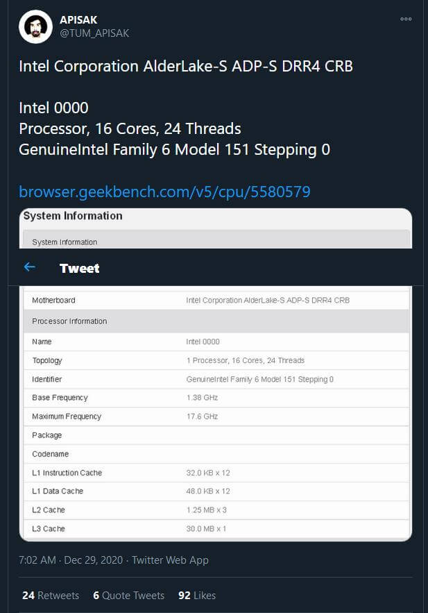
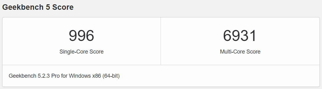
The tested platform might be supporting the new LGA 1700 socket motherboard, and was equipped with 16 GB of memory. Taking into account this is an early ES chip with very low clock frequencies; the CPU scored 996 points in single-core and 6931 points in the multi-core bench.
This particular engineering sample that is spotted features a total of 16 cores and 24 threads. So the actual CPU configuration consists of 8 Golden Cove cores with 16 threads, and 8 Gracemont cores with 8 threads. There are a total of 8 big cores and 8 small cores.
Alder Lake processors have been confirmed before to support a new LGA 1700 socket as well, as shown below.
As the name implies, the LGA1700 socket is comprised of 1,700 pins, which gives us 500 more pins that the existing LGA1200 socket that houses Comet Lake-S and the upcoming Rocket Lake-S series of processors. The upcoming LGA1700 socket board will have support for three generations of CPUs.
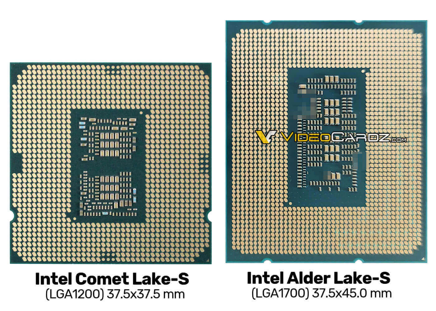
We can see that the socket dimensions for LGA1700 are 37.5mm x 45mm, which is about 7.5mm taller than Intel’s current LGA1200 socket. The bigger size is to house larger core counts than the Rocket Lake-S lineup which are currently planned for release in the first quarter of 2021, as also confirmed by Intel on its official blog.
From the picture we can see the Alder Lake CPU having a more rectangular shape, a new larger form factor, whereas the LGA1200 socket is square shaped. So Alder lake processors won’t be compatible with existing Motherboard chipsets, as they will require a new socket LGA1700 Motherboard.
The land grid array pin layout remains the same as evident from the die picture, and there are a total of 1700 gold contact pads as well.
As I said before, Alder Lake CPU lineup will bring the concept of heterogeneous multi-core to x86 processors for client PCs. High-end Alder Lake CPUs are expected to have up to 16 cores. And we’ve already seen one Alder Lake-S CPU sample sporting 16 physical cores and 32 threads before as well.
The next-gen Alder Lake-S CPUs will use a new Hybrid Core/Atom processor architecture. These next-gen CPUs are expected to support the DDR5 memory and PCIe 5.0 interface.
Just to recap some of the previous findings/leaks on Alder Lake Platform specs.
Back in July, a new GNU compiler update was posted by Phoronix, which included a list of compatible instructions for both Intel’s upcoming data center/HPC Sapphire Rapids chips and the Alder Lake desktop chips. According to the GNU update Alder Lake-S CPU lineup was noticeably missing full support for the AVX-512, a SIMD instruction recently introduced by Intel for its desktop chips.
These instruction sets are also disabled in Intel’s latest hybrid Lakefield chips. This is done to keep the instruction set more consistent between cores (small Atom Tremont cores lack support for AVX instructions though). This also eases the operating system scheduling routines that target different workloads at the corresponding cores.
Therefore, the lack of AVX-512 support for Alder Lake-S serves as further evidence that Intel will bring a new hybrid core architecture design to desktop PCs.
However, it should be noted that while the lack of AVX-512 support hints at a hybrid design, the Alder Lake ‘support matrix’ has a listing of standard AVX instructions that are not supported by the current generation Atom Tremont cores. So this means that the next generation of Atom Gracemont cores, which are largely considered ‘small’ cores used in Alder Lake, could bring AVX support, albeit in a limited manner.
The Sapphire Rapids chips on the other hand support many AVX instructions, like for example AVX512F, CLWB, AVX512VL, AVX512BW, AVX512DQ, AVX512CD, AVX512VNNI, and the new AVX512BF16 that enables support for bfloat 16, which is a compact numerical format having similar performance to FP32, but with only half the bits.
The Alder Lake-S CPU architecture will also feature the CLDEMOTE ‘cache line demote instruction’ set, which I’ve explained in my previous article. Though, to reiterate, the CLDEMOTE instruction hints to hardware that the cache line that contains the linear address should be moved (demoted) from the cache(s) closest to the processor core to a level more distant from the processor core.
CLDEMOTE instructions are used so that the OS can tell the processor core which specific line in the cache is no longer needed, and its contents can be moved elsewhere, however, not directly into the main operating memory, but still into the processor cache, at higher levels (from L1 to L2 and from L2 to L3).
Also, according to one recent report posted by Zhihu, the new hybrid Technology in the upcoming Alder Lake architecture would allow both CPU cores (small and big) to share the same instruction set and registers, but the actual availability of certain instructions would depend on which core is actually enabled and active.
The user also shared a screenshot from Intel’s internal document which suggests that the following AVX-512, TSX-NI, and the FP16 instruction sets will be disabled when the Hybrid Technology is enabled (both Big and Small cores are enabled at the same time).
The instructions will only work when the hybrid technology is disabled, which means the Small cores are disabled. By disabled we can think of the processor’s mode/PL state, though I need more technical info to confirm how this will work on Desktop PCs.
Both the big and small cores will have the same amount of instruction sets and model-specific registers, but will have different computational powers, and the overhead will also differ.
We can assume the big cores to have higher throughput and clock speeds, whereas the small cores are going to be more power efficient. Like mentioned before, the following instruction sets, e.g. AVX512, Intel TSX and FP16, are only going to work on the Big cores. ARM’s Big/Small core architecture makes more sense for mobile devices, to conserve power, but we still don’t know how this Hybrid technology is going to actually work on Desktops.
Intel has not announced any exact launch date for Alder Lake-S processors yet, but since the Alder Lake-S is the successor to Tiger Lake, so the processors will debut as the 12th Generation Core lineup next year, second half of 2021.
Stay tuned for more!
Hello, my name is NICK Richardson. I’m an avid PC and tech fan since the good old days of RIVA TNT2, and 3DFX interactive “Voodoo” gaming cards. I love playing mostly First-person shooters, and I’m a die-hard fan of this FPS genre, since the good ‘old Doom and Wolfenstein days.
MUSIC has always been my passion/roots, but I started gaming “casually” when I was young on Nvidia’s GeForce3 series of cards. I’m by no means an avid or a hardcore gamer though, but I just love stuff related to the PC, Games, and technology in general. I’ve been involved with many indie Metal bands worldwide, and have helped them promote their albums in record labels. I’m a very broad-minded down to earth guy. MUSIC is my inner expression, and soul.
Contact: Email