
One engineering board PCB picture was recently shared on Twitter allegedly claiming that the board design is for a custom Big Navi 21 GPU variant based on the new RDNA 2 architecture. The original Tweet has since been deleted though.
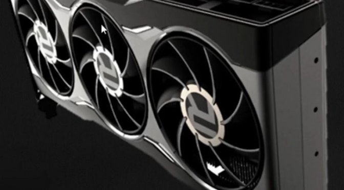
This appears to be an engineering sample PCB in early evaluation phase as evident from the board’s current layout. This likely appears to be one of the custom RX 6800 XT GPU models. The final design is going to vary since this is an engineering board sample.
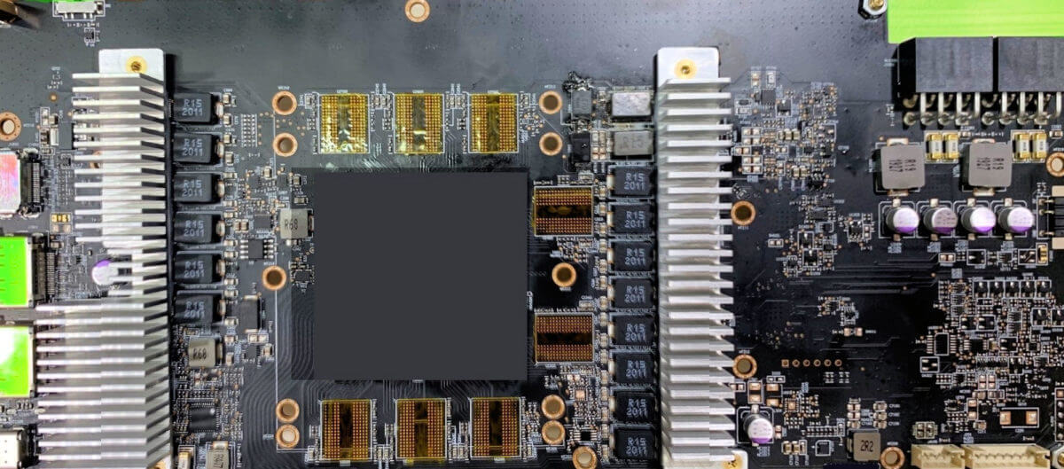
Looking at the PCB prototype there are some missing memory modules as well. Two large aluminum fin-based oversized heatsinks can also be seen covering the VRMs.
VRM stands for voltage regulator module. GPUs use VRMs to control and lower the voltage (V) sent to these components in order to avoid exceeding their maximum voltage capabilities. VRMs are especially important for overclocking a CPU or GPU.
Theoretically, VRMs should mean the power supplied to the component is consistent and steady. VRMs are buck connectors, meaning they are DC-to-DC power converters.
Since the GPU area has been blacked out by the user we cannot see the graphics processor itself. The engineering board also features a 16-phase delivery system, and two 8-PIN PCIe/PEG power connectors. One Twitter user also teased a similar reference engineering sample Navi 21 PCB before having two 8-pin connectors.
There are at least four display outputs in this board, two DisplayPort, a single HDMI port, and a USB Type-C VirtualLink connector, which was rumored before as well. 8 GDDR6 memory modules surround the GPU area as evident from the above photo, which means the Memory bus interface is 256-bit.
AMD might be using some denser DRAM modules with the Big Navi lineup, instead of dual-sided Memory, since the previously leaked PCB picture didn’t show any GDDR6 memory chips on the back of the board. There’s also a BIOS switch that can be seen on the top of the PCB.
From the board picture we can see Kapton Tape used over the memory pins, and some manual soldering done on the VRM (manual soldering on the two terminal SMD devices to the upper right of the GPU, to be precise). So this appears to be a prototype PCB.
Speaking of RX 6000 Big Navi GPU, one twitter user @CapFrameX has reported that AMD’s Navi 21 card delivers a score of 11,500 points in the 3DMark Firestrike Ultra benchmark. The card appears to be 8.5% faster than the GeForce RTX 3080 which shows the performance uplift the new RDNA 2 GPU architecture has to offer.
Firestrike Ultra
Big Navi: 11500
RTX 3080: 10600— CapFrameX (@CapFrameX) October 22, 2020
Some power consumption figures and memory specs of AMD’s upcoming Big Navi 21 GPU lineup were also reported before by Igor’s Lab. According to Igor, AMD’s RX 6000 Big Navi 21 XT flagship GPU will allegedly feature a total of 320W TBP, and 16Gbps of GDDR6 VRAM.
Igor has also pointed out that the Radeon RX 6000-series Navi 21 graphics card will use Samsung’s 16 Gbps memory modules, though AIBs are free to put a different memory if they want, as long as it is a 16 Gbps module.
Some alleged specs of AMD’s upcoming Radeon RX 6000-series NAVI 21 and NAVI 22 GPU lineup were also recently shared. More details can be found here. AMD has also issued some preventive measures to retailers to circumvent the scalping of Radeon RX 6000-series RDNA 2 GPUs.
RDNA 2 GPUs are expected to be fabbed on an optimized 7nm process node, and they will support hardware-level ray tracing as well, and are expected to deliver a 50% increase in performance per watt over previous-gen RDNA arch.
Along with an improved performance-per-clock (IPC), and logic enhancement that helps reduce the design complexity and switching power. The GPU clock speeds are also going to get a boost.
AMD plans to showcase its Radeon RX 6000 NAVI GPU lineup on October 28th, based on the new RDNA 2 architecture. John will cover this live event showcase.
Stay tuned for more!
Hello, my name is NICK Richardson. I’m an avid PC and tech fan since the good old days of RIVA TNT2, and 3DFX interactive “Voodoo” gaming cards. I love playing mostly First-person shooters, and I’m a die-hard fan of this FPS genre, since the good ‘old Doom and Wolfenstein days.
MUSIC has always been my passion/roots, but I started gaming “casually” when I was young on Nvidia’s GeForce3 series of cards. I’m by no means an avid or a hardcore gamer though, but I just love stuff related to the PC, Games, and technology in general. I’ve been involved with many indie Metal bands worldwide, and have helped them promote their albums in record labels. I’m a very broad-minded down to earth guy. MUSIC is my inner expression, and soul.
Contact: Email