
It appears that Yangtze Memory Technologies Co., Ltd. (YMTC) is helping push China’s self-sufficiency, and its domestic market. 3D Xtacking NAND devices are being manufactured from Yangtze Memory Technologies Co., Ltd. (YMTC) in Wuhan, China. With this move, YMTC has become China’s first mass-producer of 3D NAND flash memory chips.
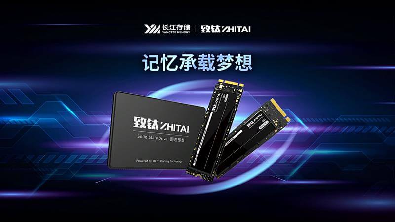
The chipmaker has recently launched the two new SSDs, the PC005 and the SC001, under the ZHITAI sub-brand. These SSDs use 64-layer 3D NAND chips that are manufactured with the Xtacking 3D NAND technology. This 64L 3D NAND flash device represents the first major competitive semiconductor product to come out of China’s state-backed investment in cutting-edge memory chips. There is no question that this will disrupt the 52?billion dollar NAND memory market, and also its respective market leaders such as Samsung, Kioxia, Western Digital, Micron, Intel, and SK hynix.
YMTC’s 64L 3D NAND device is a disruptor not only because it is offered by a significant new entrant, but because of its Xtacking architecture. YMTC is already on track for 128-layer QLC (quad-level cell) 3D NAND offerings that max out at 1.6 Gbps. This was revealed back in April. Given YMTC’s recent collaboration with ‘Phison’, we can assume that the drives are using a Phison controller, though it can be a custom controller from ‘Silicon Motion’ as well.
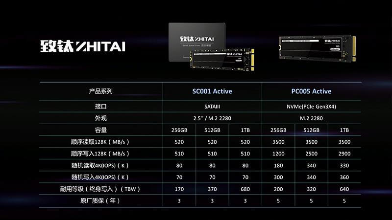
YMTC currently offers two SSD models, the PC005 and SC001 active, both having capacities of 256GB, 512GB and 1TB, respectively. The PC005 has a limited five-year warranty, whereas the SC001 has a shorter three-year warranty given by the company. The PC005 Active is a standard M.2 2280 model that makes use of the PCIe 3.0 x4 interface. The sequential read and write speeds have been rated for 3,500 MBps and 2,900 MBps, respectively.
The PC005 Active SSD Model offers random performance up to 340,000 IOPS reads and 360,000 IOPS writes. Endurance hovers between 200 TBW and 640 TBW. The SC001 Active SSD, on the other hand, is available in both M.2 2280 and 2.5-inch formats. But this drive will be limited to SATA III interface speeds nonetheless. YMTC claims sequential read and write speeds up to 520 MBps and 510 MBps, respectively, and random read and write speeds up to 80,000 and 70,000 IOPS (for all capacity models). The endurance varies from 170 TBW to 680 TBW.
These drives from YMTC may offer similar performance to other drives currently in the market, such as those from Samsung. For an example, the PC005 Active 1TB model’s sequential numbers surpass the Samsung 970 Evo 1TB’s rating. Though, the Samsung drive is way ahead than the PC005 in random performance. However, the PC005 Active 1TB’s endurance is rated for 640 TBW, which is 40 TBW higher than the Samsung 970 Evo 1TB model.
We can compare the SC001 Active 1TB’s sequential performance with Samsung 860 Evo 1TB SSD’s rated figure. Though, in random performance, Samsung is again ahead. But the endurance rating of the SC001 Active 1TB is 680 TBW, while the Samsung 860 Evo 1TB only has 600 TBW rating.
Coming to the technology, analysis of YMTC 3D 64L Xtacking TLC NAND devices, found in the UNIC Memory Secure S1-C 64 GB USB, shows 73 gates in total for a vertical NAND string with nine vertical channel (VC) holes including one dummy hole between common source line contacts. It is likely that 4 select gates (1 GST and 3 SSTs) and 5 dummy gates are also used.
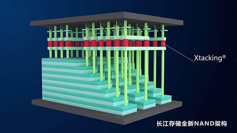
Due to Xtacking architecture in which periphery circuits and memory cell operations are processed on a separate wafer, the array efficiency and memory bit density are considerably higher than conventional 3D NAND such as Samsung 64L V-NAND and KIOXIA/WD 64L BiCS NAND. For example, YMTC 64L 256 Gb die bit density is 4.41 Gb/mm2 which is higher than Samsung 64L 256 Gb die (3.42 Gb/mm2), and comparable to Micron/Intel 64L CuA FG 256 Gb TLC die (4.40 Gb/mm2) The NAND memory array efficiency on the die for YMTC 64L shows more than 90 %.
Since YMTC Xtacking uses Wafer-to-Wafer bonding technology, the NAND array is upside-down on periphery circuits. The process integration consists as (1) Metal 1 through Metal 4 for periphery circuits on a wafer, (2) NAND array with a source plate (SP) and Metal 1’ through Metal 3’ on a separate wafer, (3) Wafer-to-Wafer bonding to connect M4 and Metal 3’, (4) Through SP Via and Metal 5. Here, Metal 1’ is for BL.
NAND array consists of the same number of total gates compared to KIOXIA/WDC BiCS 64L 3D NAND. Bit-line half pitch for the device is 20 nm, which means they use a double patterning technology (DPT) likely with self-aligned double patterning (SADP). They do not use any type of metal straps to connect bit lines with NAND channels, which is different from Samsung’s 64L V-NAND array structure. Top select gate (TSG) cut process is also used on array.
The Chinese online retailer JD.com is currently selling the PC005 Active 256GB and 512GB models for around $54 and $77. 1TB pricing is not listed yet. SC001 Active 256GB, 512GB and 1TB models are listed for $42, $67 and $123, respectively. These SSD models come in 2.5-inch form factor.
Thanks PC Watch
Hello, my name is NICK Richardson. I’m an avid PC and tech fan since the good old days of RIVA TNT2, and 3DFX interactive “Voodoo” gaming cards. I love playing mostly First-person shooters, and I’m a die-hard fan of this FPS genre, since the good ‘old Doom and Wolfenstein days.
MUSIC has always been my passion/roots, but I started gaming “casually” when I was young on Nvidia’s GeForce3 series of cards. I’m by no means an avid or a hardcore gamer though, but I just love stuff related to the PC, Games, and technology in general. I’ve been involved with many indie Metal bands worldwide, and have helped them promote their albums in record labels. I’m a very broad-minded down to earth guy. MUSIC is my inner expression, and soul.
Contact: Email