
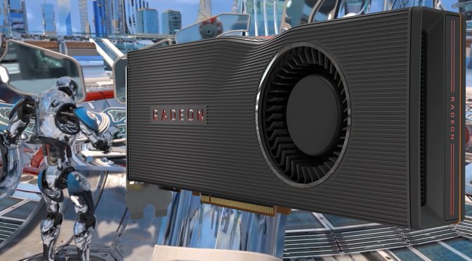
AMD has been quite successful with its chiplet-based design which the company has used in its recent Zen series of processors. Instead of building standard, monolithic CPUs, AMD opted for a new type of configuration called a chiplet. From a marketing perspective, chiplets have been a huge hit.
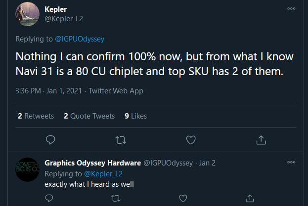
Now there is some chatter on the web that AMD’s upcoming flagship Navi 31 graphics processor might be the first GPU to use the MCM (multi-chip module) approach and design, and this chiplet design is supposed to feature two 80 Compute Unit (CU) dies. This doesn’t come as a surprise because AMD has already submitted a new patent for an MCM “GPU chiplet” design before.
This leak comes via Twitter user @Kepler_L2, and according to him AMD’s next-gen Navi 31 GPU will have a dual chiplet design with 80 Compute Units each. This means that there are going to be 160 CUs in total, twice as many as the current Navi 21 GPU variant.
A two 80 CU die would bring the total number of cores to 10240, two times 5120 cores found on the Navi 21 die. AMD has already promised before that the RDNA 3 GPU architecture is going to bring a huge leap in compute performance, and better performance-per-watt compared to the previous generation of cards.
For RDNA 3, AMD would be leveraging a more advanced process fabrication node, and will use Infinity Cache in a more proficient way.
According to AMD, current RDNA 2-based Radeon RX GPUs deliver a 50% perf per watt improvement over their predecessors, and AMD promises us to expect similar gains with the third generation RDNA GPU architecture as well.
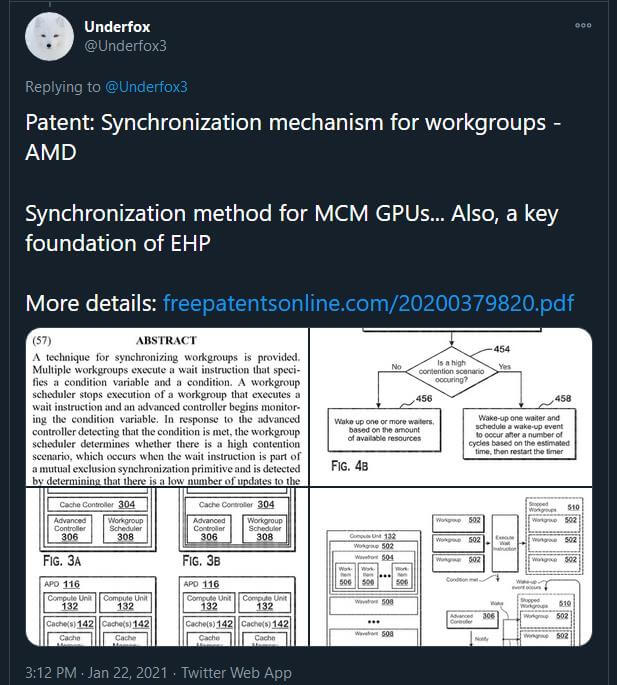
On some other related news, Twitter user @Underfox3 points out that AMD has a new patent in works, and the document highlights that the red team is developing a technology to synchronize the overall workload between MCM based GPUs, with its future architectures.
One Patent is titled as, “Synchronization mechanism for workgroups”, which happens to be a synchronization method for an MCM GPU design which AMD might implement with RDNA3 and future GPU architectures.
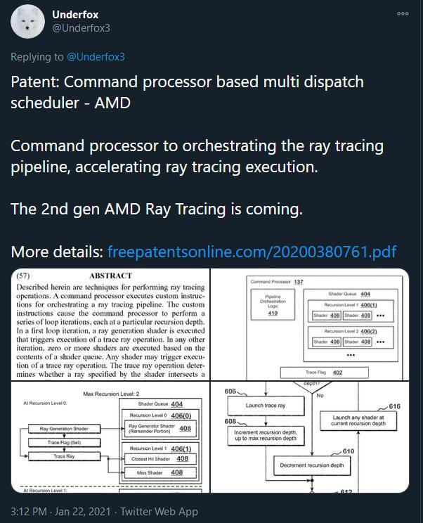
The other Patent titled as “Command processor based multi dispatch scheduler”, basically describes how a command processor can orchestrate the ray tracing pipeline, and thus accelerate ray tracing execution. The patent also mentions 2nd gen AMD Ray Tracing support.
AMD has already assured its future next-gen Zen 4/Zen 5 Ryzen CPUs and RDNA 3-based GPUs are on track. It would be interesting to see how AMD takes this MCM approach with its future lineup of gaming GPUs.
NVIDIA is also rumored to use an MCM approach with its next-gen “Hopper” GPU lineup, but we don’t know whether the Hopper arch is going to be end up in consumer gaming cards or not.
Nvidia still has the upper hand when it comes to hardware accelerated Ray tracing performance, and it remains to be seen how AMD can compete on this front. AMD also needs to give an answer to Nvidia’s own DLSS AI-based super-resolution technology.
AMD already has experience with a multi-chip design with the Ryzen CPU lineup and various APUs, and NVIDIA and Intel will both have their own GPU chiplet-style architectures in the coming years as well.
According to AMD the conventional “monolithic” die designs are becoming increasingly expensive to manufacture, so the company plans to adopt a new GPU chiplet design. Due to the high latency between chiplets, an MCM approach was dropped in favor of a Monolithic design.
We can also expect massive yield gains from just shifting to an MCM based approach instead of a monolithic design. Despite having very poor yields, a single huge die was expensive to produce, and wastage was also an issue.
On Monolithic designs, the GPU programming model is often inefficient because the parallelism is difficult to distribute across multiple different working active groups and chiplets. It is also expensive design-wise to synchronize the memory contents of shared resources throughout the entire system, to provide a coherent view of the memory to applications.
Additionally, from a logical point of view, applications are written with the view that the system only has a single GPU. That is, even though a conventional GPU includes many GPU cores, applications are programmed as addressing a single device.
So, it has been historically challenging to bring chiplet design methodology to GPU architectures.
According to AMD such problems can be avoided by implementing a high bandwidth “passive crosslink”, which is basically an on-package interconnect.
The first GPU chipset would be directly communicably coupled to the CPU, while each of the GPU chiplets in the array would then be coupled to the first GPU via a passive crosslink.
To improve system performance by using GPU chiplets while preserving the current programming model, AMD illustrated systems that will utilize high bandwidth passive crosslinks for coupling GPU chiplets.
The said system includes a central processing unit (CPU) communicably coupled to a first graphics processing unit (GPU) chiplet of a GPU chiplet array. Basically the array includes the first GPU chiplet communicably coupled to the CPU via a bus, and a second GPU chiplet communicably coupled to the first GPU chiplet via a passive crosslink.
The passive crosslink is a passive interposer die dedicated for inter-chiplet communications. AMD plans to use a passive crosslink for communication between GPU chiplets, which are all on a single interposer.
This could mean that groups of GPU chiplets act like a System-on-a-Chip (SoC) which is divided into separate and different functional chips. This new chiplet design appears to suggest that each GPU chiplet will be a GPU in its own right and fully addressable by the operating system/OS as well.
Stay tuned for more tech news!
Hello, my name is NICK Richardson. I’m an avid PC and tech fan since the good old days of RIVA TNT2, and 3DFX interactive “Voodoo” gaming cards. I love playing mostly First-person shooters, and I’m a die-hard fan of this FPS genre, since the good ‘old Doom and Wolfenstein days.
MUSIC has always been my passion/roots, but I started gaming “casually” when I was young on Nvidia’s GeForce3 series of cards. I’m by no means an avid or a hardcore gamer though, but I just love stuff related to the PC, Games, and technology in general. I’ve been involved with many indie Metal bands worldwide, and have helped them promote their albums in record labels. I’m a very broad-minded down to earth guy. MUSIC is my inner expression, and soul.
Contact: Email