
TSMC or Taiwan Semiconductor Manufacturing Company Ltd is a Taiwanese multinational semiconductor contract manufacturing and design firm. It is one of Taiwan’s largest companies, the world’s most valuable semiconductor company, and the world’s largest dedicated independent (pure-play) semiconductor foundry.
According to a press report coming via Nikkei Asia, TSMC is drawing attention to the growing importance of chip packaging, a little-known part of the process of making semiconductors.
Silicon manufacturing these days can be quite challenging, and it requires massive investment, and extensive knowledge of the silicon process technology, and how it works.
NIKKEI Asia source reports that TSMC aims to work with Google, AMD and other U.S. tech giants to develop a new way of making semiconductors more powerful. TSMC plans to push the production of 3D chip manufacturing process.
With the advancement in silicon tech, MOORE’s Law has actually slowed down, as it has become more difficult to shrink the space between transistors and thus fit more onto a chip.
Moore’s Law is the observation made in 1965 by Gordon Moore, co-founder of Intel, that the number of transistors per square inch on integrated circuits had doubled every year since the integrated circuit was invented. Moore predicted that this trend would continue for the foreseeable future.
In subsequent years, the pace slowed down a bit, but data density has doubled approximately every 18 months, and this is the current definition of Moore’s Law, which Moore himself has blessed. Most experts, including Moore himself, expect Moore’s Law to hold true until 2020-2025.
But the traditional approach of cramming and putting ever more transistors onto a single chip is starting to slow down and lose steam. Chip packaging is one of the final steps in the chipmaking process, in which semiconductors are mounted into a supportive case before being placed on a print-circuit board.
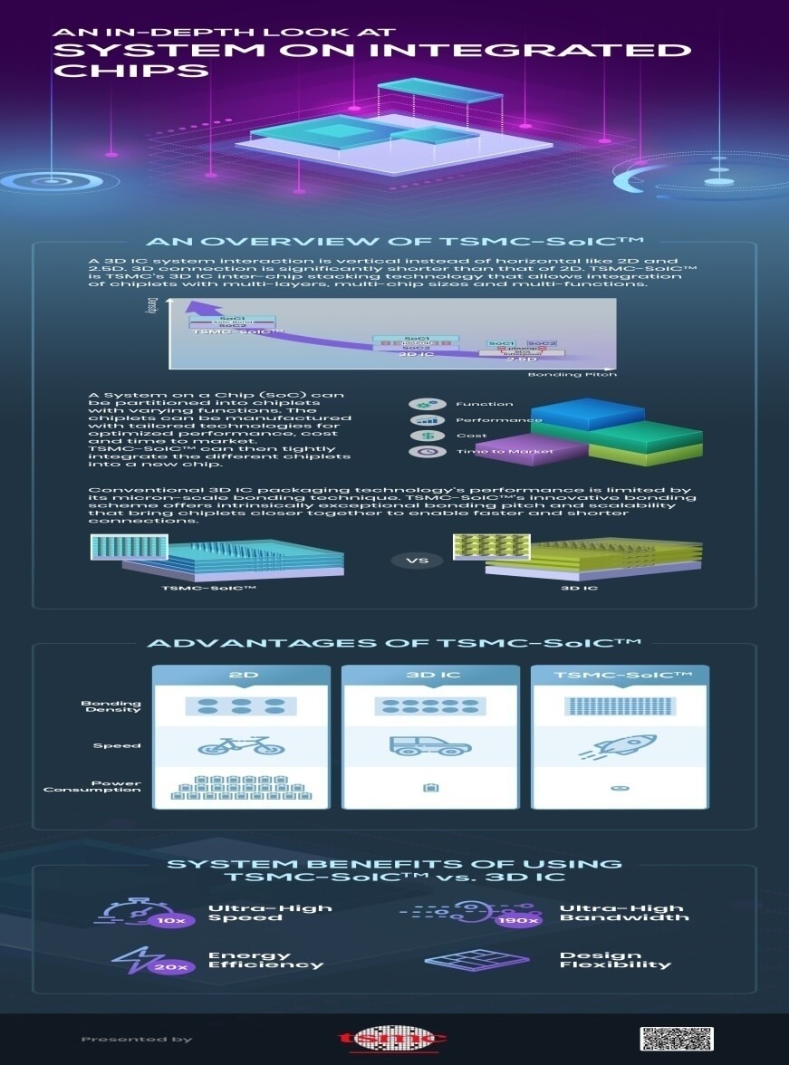
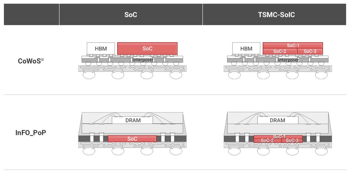
But TSMC is now taking chip packaging vertically and horizontally, using a new 3-D technology that is dubbed as SoIC. It makes it possible to stack and link several different types of chips, such as processors, memory and sensors, all into one whole package, according to the company. This approach makes the whole chipset smaller, more powerful and more energy-efficient.
TSMC-SoIC service platform provides innovative front-end, 3D inter-chip (3D IC) stacking technologies for re-integration of chiplets partitioned from System on Chip (SoC). TSMC will deploy the 3D silicon manufacturing technology at its chip packaging plant in Taiwanese city of Miaoli.
Google and AMD will be among its first customers for SoIC chips, and are helping TSMC to test and certify this technology. Construction on the plant is slated for completion next year, with mass production to begin in 2022.
As per one chip packaging industry insider expert, “TSMC is of course not trying to replace all traditional chip packaging players, but it aims to serve those premium clients at the very top of the pyramid so those deep-pocketed chip developers like Apple, Google, AMD and Nvidia won’t leave TSMC for its competitors”.
“These new chip stacking techs require advanced chip manufacturing expertise as well as a lot of computer simulations to achieve precise stacking, so it’s very difficult for traditional chip packaging providers to step in”.
TSMC is not the only chipmaker investigating the possibilities of more advanced chip packaging tech. Small rivals like SMIC/Semiconductor Manufacturing International Co., which is China’s biggest contract chipmaker, is looking at building a similar advanced chip packaging tech.
“We expect revenue from our backend services, which include both advanced packaging and testing to grow at a rate slightly above the corporate average in the next few years,” TSMC CEO and Vice Chairman C.C. Wei said in an earnings briefing in mid-October.
Google plans to use chips made with the SolC process for autonomous driving systems and other applications. Google is a relative newcomer in designing its own chips, which it currently uses for artificial intelligence/AI computing in its data center servers.
AMD, which develops microprocessors for computers and servers, is also eager to take advantage of the latest stacking technologies in hopes of creating chip products capable of outperforming those of its bigger rival which is Intel.
TSMC already has a chip packaging plant in the Taiwanese city of Taoyuan, mainly serving Apple’s needs. Besides Taoyuan and Miaoli, TSMC is also building a chip packaging plant in the southern Taiwanese city of Tainan near its most advanced 5-nanometer chip plant, dubbed Plant 18, which is still expanding to later churn out even more advanced 3-nanometer chips.
Arisa Liu, a semiconductor analyst with Taiwan Institute of Economic Research, said the demand for advanced packing is growing, as premium chip developers worldwide seek more customized chips that can generate powerful performance and help them stand out from their rivals.
“It has become a new arena for leading chip manufacturers TSMC, Samsung and Intel, as well as for global leading chip developers,” Liu said. “It’s also viewed as a means to counter the slowing of Moore’s Law.”
Stay tuned for more!
Hello, my name is NICK Richardson. I’m an avid PC and tech fan since the good old days of RIVA TNT2, and 3DFX interactive “Voodoo” gaming cards. I love playing mostly First-person shooters, and I’m a die-hard fan of this FPS genre, since the good ‘old Doom and Wolfenstein days.
MUSIC has always been my passion/roots, but I started gaming “casually” when I was young on Nvidia’s GeForce3 series of cards. I’m by no means an avid or a hardcore gamer though, but I just love stuff related to the PC, Games, and technology in general. I’ve been involved with many indie Metal bands worldwide, and have helped them promote their albums in record labels. I’m a very broad-minded down to earth guy. MUSIC is my inner expression, and soul.
Contact: Email