
During a recent virtual 2020 Flash Memory Summit, CEO and founder of NEO Semiconductor, Andy Hsu, gave us a detailed insight on the company’s new X-NAND flash architecture that aims to combine the speed of an SLC flash with the capacity/density and low pricing of the QLC NAND flash.
NEO Semiconductor is a startup company focused on 3D NAND flash memory, 3D emerging memory, and IoT memory. The company was founded in 2012 by Andy Hsu and a team in San Jose, California. The company currently owns 20 U.S. patents in memory design architectures and cell structures.
In 2018, the company made a breakthrough in the world’s fastest 3D NAND architecture dubbed as X-NAND. X-NAND can achieve SLC’s speed with TLC and QLC densities. This provides a high-speed, low-cost solution for not only PC gamers and enthusiasts, but also for 5G, AI/ML, real-time analysis, VR/AR, cyber security/NAS, and many industrial and commercial applications.
The company also recently won the Best of Show Award – “Most Innovative Flash Memory Startup”.
NEO claims X-NAND is the future architecture of 3D NAND, thus resulting in a QLC NAND with read/write performance comparable to that of an SLC NAND. In case you didn’t know, as traditional NAND technologies have developed, the increase in the CELL density comes at the cost of write endurance and performance.
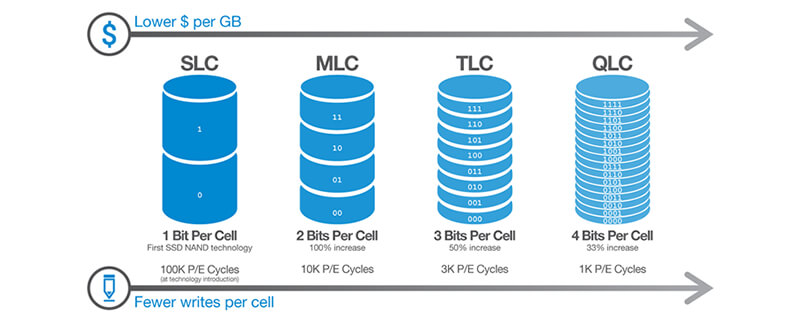
QLC NAND might offer clients an excellent value for money, but it can also deliver poor write speeds without having the assistance of SLC caching. With time PLC (5 bits per cell) NAND will also become available in the market, making these write performance/endurance problems worse.
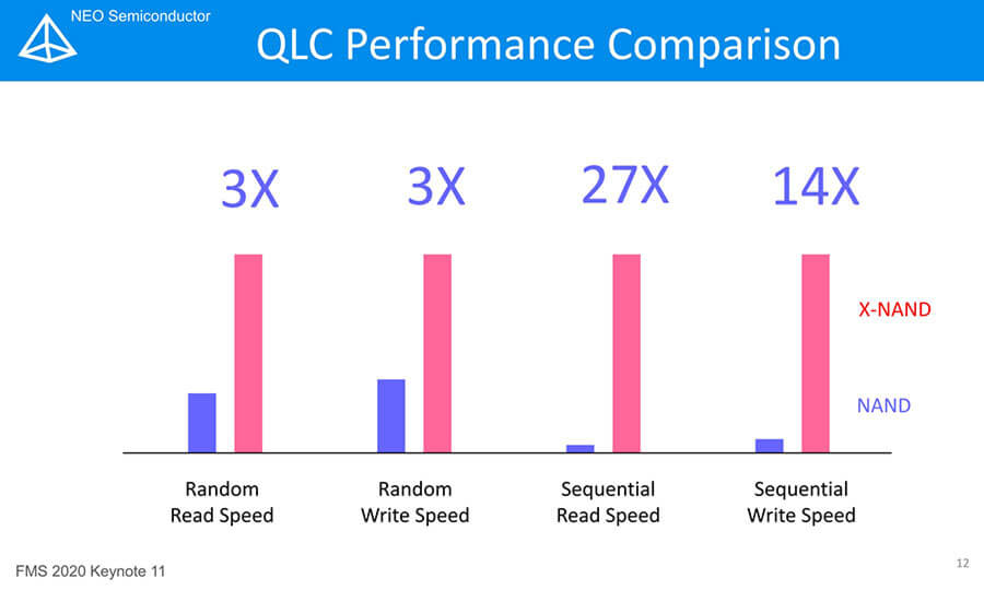
NEO Semiconductor claims X-NAND can do random read and write workloads 3x times faster than the QLC flash. X-NAND can also offer 27x/14x times better sequential read/write workloads.
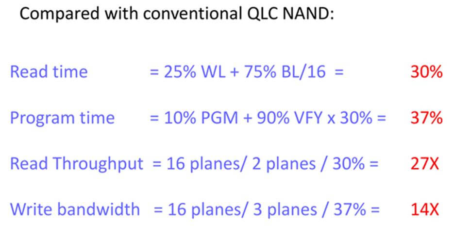
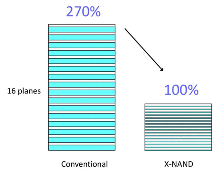
These performance figures are achieved with a much smaller die that’s roughly 37-40% the size of a 16-plane design, as shown in this diagram. Though, please note that the speed and die size reduction can be balanced as needed.
You can think of this new tech basically as a ‘best of both worlds’ solution by delivering QLC-like levels of storage density, while also offering a 4x increase in read performance and an 8x increase in write throughput.
QLC can actually be too slow for some of the Industrial/enterprise applications, if not all, that may require very high-speed storage access. Some tech companies have tried to address this issue by employing DRAM and SLC cache, but Neo Semi’s technology X-NAND takes a totally new and different approach.
Assuming this new NAND technology is properly utilized, we can get higher speed SLC-like NAND memory in the market.
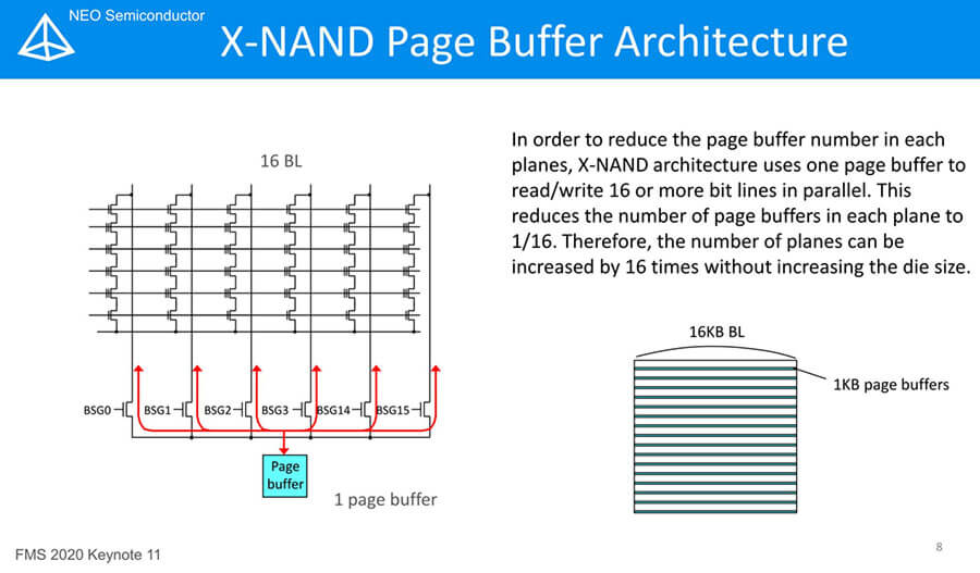
Below you can see the X-NAND Page BUFFER architecture. As you can see X-NAND will use 1 page buffer to read/write at least 16 bits in parallel mode. The Page buffer is also reduced as well.
NEO semiconductor plans to release a working “prototype chip” to demonstrate this tech in time, so that NAND manufacturers can also implement its patented design in existing processes.
Recently, in the NAND market we have moved to cheaper but slower flash to increase the density, for example, from 3-bit TLC to 4-bit QLC, but at what cost? The performance and endurance both have been compromised to an extent. And, Sequential write performance has also been reduced, because of the increased Read and write latencies.
X-NAND will offer a way for the flash to maintain SLC performance throughout by allowing for simultaneous SLC and QLC write modes.
To quote NEO Semiconductor:
“QLC 3D NAND flash has already found many applications due to its higher density and lower price than other NAND types. However, a serious limitation is that QLC has relatively low performance, especially write speed. NEO Semiconductor has developed a new architecture called X-NAND, which can increase QLC NAND’s read speed by 4X and write throughput by 8X.
That results in QLC NAND with read/write performance comparable to SLC NAND.
X-NAND architecture can produce the high-speed, low-cost solution required by such emerging applications as AI/ML, 5G, real-time analysis, VR/AR, and cybersecurity. X-NAND architecture can be applied to SLC to PLC flash. Simulation shows that X-NAND in SLC can increase read speed by 10X and deliver an astonishing read throughput of 85 GB/s. The architecture enables NAND flash to be readily integrated into ultra-high-bandwidth 3D integrated chips.”
As per Andy Hsu higher-density flash is growing at a very rapid rate, and the company anticipates that almost 40-50% of the NAND market would be comprised of QLC by 2024. Furthermore, X-NAND programming and erase policies are designed to significantly improve endurance over QLC flash.
As note before, X-NAND can easily achieve these gains by going from a 16KB page buffer per plane to a 1KB page buffer per plane, but with sixteen times the planes. X-NAND can work with any number of existing NAND layouts, which in the end can increase the design flexibility and also the ease of conversion, to some extent.
Technically speaking, let me make this clear that X-NAND has six primary attributes: “multiple bit line writes, multi-plane QLC programming, program suspend, multi-BL reads, single latch QLC reads, and the SLC/QLC parallel programming”.
So based on this, the program throughput can be improved as multiple planes can be used in the programming sequence. But this all depends on the end implementation. So the current use of multiple banks will allow for simultaneous SLC and QLC programming.
Doing this will signal and make sure that the SLC pages are never full, however the data can be programmed to the QLC pages at SLC speed. This is what X-NAND actually aims to deliver.
This new X-NAND technology will take few more years to be adopted by the industry. But it surely provides an alternative and incentive for SSD makers.
Faster storage solutions will surely come to market with time, and technologies like X-NAND will keep on progressing, thus marking a new era in storage drives. Technology never stops!
Stay tuned for more!
Hello, my name is NICK Richardson. I’m an avid PC and tech fan since the good old days of RIVA TNT2, and 3DFX interactive “Voodoo” gaming cards. I love playing mostly First-person shooters, and I’m a die-hard fan of this FPS genre, since the good ‘old Doom and Wolfenstein days.
MUSIC has always been my passion/roots, but I started gaming “casually” when I was young on Nvidia’s GeForce3 series of cards. I’m by no means an avid or a hardcore gamer though, but I just love stuff related to the PC, Games, and technology in general. I’ve been involved with many indie Metal bands worldwide, and have helped them promote their albums in record labels. I’m a very broad-minded down to earth guy. MUSIC is my inner expression, and soul.
Contact: Email