
Rocket Lake (RKL) is a planned microarchitecture designed by Intel as a direct successor to the Comet Lake-S series of desktop CPUs and high-performance mobile devices. These were expected to hit the market by the end of this year, but Intel’s roadmap has no mention of this.
One VLSI engineer who goes by the name ‘Retired Engineer’ on Twitter, @chiakokhua, recently tweeted one of his old findings from November 2019 last year. According to him the upcoming Rocket Lake-S processors are going to feature “multi-chip modules/MCM” of core and uncore GPU dies built on different silicon fabrication nodes.
This is speculation from his side, but he has a strong record of accurate prediction in the past, when he spoke about the 3rd gen Ryzen Matisse AM4 processors being multi-chip modules as well. Apparently, it might be possible that Intel is also designing these socket LGA1200 Rocket Lake processors to feature multi-chip modules, similar to Matisse in some ways.
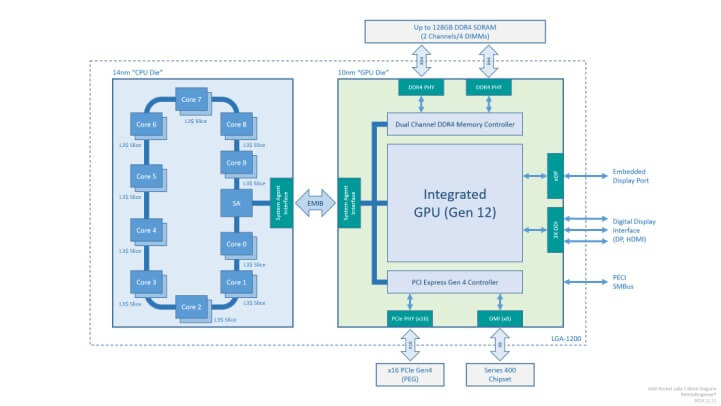
According to the block diagram posted by @chiakokhua, it appears that Rocket Lake-S is a multi-chip module consisting of a 14 nm die that holds the ‘CPU cores’; and a 10 nm die that holds the ‘uncore’ components. But in the case of Rocket Lake the uncore DIE is more advanced that the CPU die.
The CPU die is fabbed on a 14 nm node on Rocket Lake-S, which contains the ‘Willow Cove’ CPU cores in this die, and a system agent, which are connected together by a Ring-bus interconnect. And the system agent connects to the 10nm uncore GPU die via EMIB.
The 10 nm GPU uncore die on the other hand features the Gen12 XE iGPU with up to 96 EUs, a dual-channel DDR4 memory controller, a PCI-Express 4.0 controller, as well as display and media engines. Rocket Lake-S MCM provides a total of 24 PCI-Express lanes, out of which 16 are assigned as PEG (PCI-Express Graphics), and 8 lanes are assigned as chipset bus. Previous gen Comet Lake-S CPU lineup only provided 20 lanes.
This is not the first time Intel is taking the MCM approach. Clarkdale first-gen desktop processor supporting the LGA1156 package was an MCM having a 32 nm CPU die, and a 45 nm uncore graphics and integrated memory controller die. It remains to be seen whether Intel really chooses the MCM approach with the Rocket Lake- S lineup of desktop processors.
Hello, my name is NICK Richardson. I’m an avid PC and tech fan since the good old days of RIVA TNT2, and 3DFX interactive “Voodoo” gaming cards. I love playing mostly First-person shooters, and I’m a die-hard fan of this FPS genre, since the good ‘old Doom and Wolfenstein days.
MUSIC has always been my passion/roots, but I started gaming “casually” when I was young on Nvidia’s GeForce3 series of cards. I’m by no means an avid or a hardcore gamer though, but I just love stuff related to the PC, Games, and technology in general. I’ve been involved with many indie Metal bands worldwide, and have helped them promote their albums in record labels. I’m a very broad-minded down to earth guy. MUSIC is my inner expression, and soul.
Contact: Email