
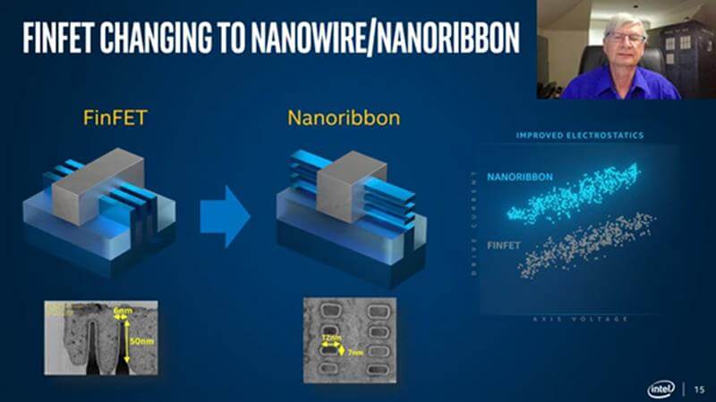
At this year’s international VLSI conference, Intel CTO Mike Mayberry revealed that the company expects to have new nanowire/nanoribbon transistors in high-volume production within the next five years. Intel is planning to move beyond its current FinFET transistor technology layouts.
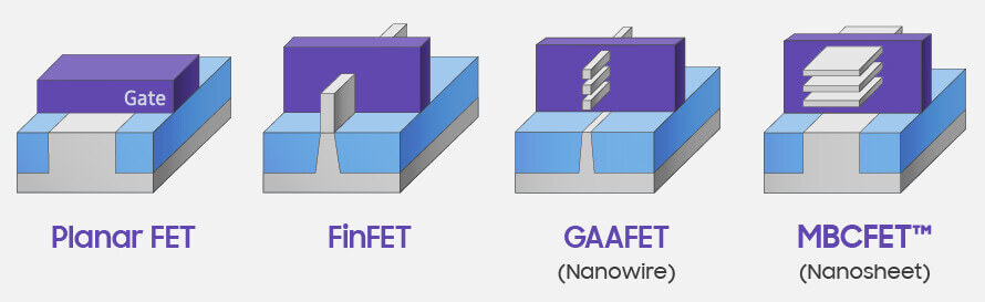
This is a form of a ‘gate-all-around’ (GAAFET) transistor, which seems to be the next big step since the introduction of FinFET. The GAA-type design will offer space savings as well as power savings at the “silicon” level. Mayberry did not provide any specifics nor spoke about Intel’s roadmap in the Q&A, but he narrowed it down by saying “within the next five years”.
Intel plans to transition to a new transistor layout called GAAFET, which will offer better efficiency and enhanced silicon performance. GAAFET used by Intel is a ‘nanoribbon’, which is a new design over the current FinFET transistors. Samsung has already revealed its own GAAFET-style transistors with their 3nm MBCFET (Nanosheet) designs, which will enter risk production in late 2020.
GAAFET takes the idea behind FinFET transistors to the next level to offer all-around (hence the name Gate-All-Around) coverage of the transistor’s channel. FinFET, simply put, places a fin within the GATE that has three out of four sides covered, whereas GAAFET transistors have all the sides covered. This improved design can help lower power loss and increase a transistor’s performance. The GAAFET transistor will power the next generation of desktop, datacenter and mobile devices.
Intel’s CTO says the company will eventually abandon the “CMOS technology” that has been used in IC fabrication for decades. The company plans to replace it with Nanowire and nanoribbon structures. In traditional IC fabrication, FETs are formed by doping a portion of the silicon die and then depositing a gate structure on top of an insulating layer parallel to the surface of the die.
Basically FinFET structures started appearing about a decade ago, in which the transistor channel rises above the whole die surface and the gate wraps around these raised “fins”. These transistors are faster and have a high current capacity than CMOS devices. However, the pressure of producing more and more sophisticated ICs will drive the move away from even the FinFET tech. The gate can surround the channel on all sides, by creating the channel in multiple flat sheets or multiple wires, leading to even better performance. It also allows for the finer tuning of the transistor characteristics in the end.
Another goal of these nanostructures is obviously density. With the fin topology, one section of the channel remains bound to the die. With the nanoribbon or wire structure, it appears as if the fin is floating and this allows the gate to surround the channel.
In 1965, Intel cofounder Gordon Moore first observed that the number of transistors that could fit onto a dense integrated circuit (or chip) doubled each year. In 1975, Moore adjusted this “Law” to approximately every two years. Since then, computing power has expanded at an astounding rate.
For instance, the Apple 1, which premiered in 1976, featured a 1MHz processor and 4 kilobytes of RAM. Today, processor speeds are measured into the multiple-gigahertz range with multiple cores, multiple gigabytes of RAM, and accessories to process data at a speed that would have been mind-boggling not long ago. These advances also allow the miniaturization of modern smartphones and any number of other devices. For the last decade, or perhaps even longer, we’ve been hearing that Moore’s Law is dead, dying, or is on some sort of life support. But this is not the case.
Regardless of how many more transistors we can fit onto a chip, engineers continue to find novel ways to optimize and take advantage of what’s available. We are still finding ways to fit more transistors onto a chip. As per an old 2014 article from ‘MIT Technology Review’, to stay true to Moore’s Law, chips would have to have features in the 5-nanometer range to keep up.
In my opinion, that’s a staggering demand, considering silicon atoms themselves are only around .2nm. However, here we are in early 2020, and limited production of 5nm trials has been completed, with mass production slated to begin this year. As predicted in the above MIT article, chips made using carbon nanotube transistors should be available in 2020. While it doesn’t look like you’ll be able to buy a “carbon computer” this year, researchers at MIT made excellent progress on this technology in 2019, creating a 16-bit microprocessor consisting of more than 14,000 carbon nanotube field-effect transistors (CNTFETs).
If we’re looking at transistors on a chip doubling every two years per Moore’s (current) Law, the six years between the 2013 and 2019 chip would predict only a 712 CNTFET processor. Doubling this rate every year would result in 11,392 transistors on a chip. Thus, CNTFET advancement has exceeded even Moore’s early prediction, an exciting development if this trend continues.
One very important aspect to overcome is that these chips typically need to be 99.999999% pure to function properly. This is actually impossible under today’s processes; however, researchers were able to design around this obstacle for the 2019 RISC CNTFET processor, allowing them to make do with only 99.99% purity. Processes have also been developed to mitigate a large number of these defects directly.
We can expect further advances as these techniques evolve, hopefully clearing the way for mainstream carbon-based computing. The advantages of Carbon Nanotube Transistors are that they are more Energy-efficient. More computing power generally equates to more power usage and challenges for heat dissipation. As it turns out, research indicates that CNTFET technology may be an order of magnitude more energy-efficient than its silicon counterparts. Carbon nanotubes are excellent at dissipating the heat they produce, a problem that plagues silicon-based computers as processors are clocked at higher and higher speeds to increase performance.
Hello, my name is NICK Richardson. I’m an avid PC and tech fan since the good old days of RIVA TNT2, and 3DFX interactive “Voodoo” gaming cards. I love playing mostly First-person shooters, and I’m a die-hard fan of this FPS genre, since the good ‘old Doom and Wolfenstein days.
MUSIC has always been my passion/roots, but I started gaming “casually” when I was young on Nvidia’s GeForce3 series of cards. I’m by no means an avid or a hardcore gamer though, but I just love stuff related to the PC, Games, and technology in general. I’ve been involved with many indie Metal bands worldwide, and have helped them promote their albums in record labels. I’m a very broad-minded down to earth guy. MUSIC is my inner expression, and soul.
Contact: Email