
AMD has already made great strides with their high performing Zen 2 and Zen 3-based lineup of processors, and now the company wants to further expand its presence in the CPU industry. The company claims it wants to improve performance not just through faster and efficient CPU cores, but also through the use of FPGAs.
AMD has recently filed a patent application for integrating FPGAs into a CPU, which would allow the processor to run certain custom instruction sets. FPGA is short for field-programmable gate array. So basically the new patent outlines a CPU design with FPGA elements integrated into its core design, and is titled “Method and Apparatus for Efficient Programmable Instructions in Computer Systems”.
The patent states that the FPGA elements will actually share some CPU resources such as registers for floating-point and integer execution units, since they can run specific instruction sets very quickly. AMD plans to design a processor that can include one or more programmable execution units that can be made to handle different types of custom instruction sets.
Field Programmable Gate Arrays (FPGAs) are semiconductor devices that are based around a matrix of configurable logic blocks (CLBs) connected via programmable interconnects. FPGAs can then be reprogrammed to desired application or functionality requirements after manufacturing.
This feature distinguishes FPGAs from Application Specific Integrated Circuits (ASICs), which are custom manufactured for specific design tasks. A standard x86 CPU core is basically designed to run a variety of instruction sequences, sometimes even slowly.
So suppose if there’s a specific task that is used on a regular basis, then it might be beneficial to create a custom instruction on an FPGA that will process the code much more quickly. The task can be anything, like e.g. graphics, physics, AI inferencing and acceleration, AVX, video hardware acceleration, and other workloads etc.
Apart from that, FPGAs can be re-programmed on the fly to run another instruction set if need be. So technically speaking they aren’t limited to a single instruction set.
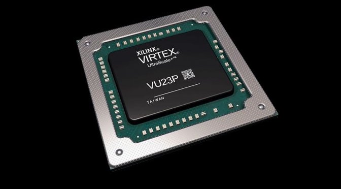
This patent comes as a result of when AMD made its largest acquisition to date last year in October, in which the company announced acquisition plans for Xilinx, a firm which specializes in FPGAs. Xilinx was founded in 1984 and the company is well known for its FPGA (field programmable gate array) chips, programmable system-on-chips (SoCs), and adaptive compute acceleration platform (ACAP).
Xilinx products are used in everything from “consumer” items to aerospace and defense technology.
AMD’s new design implementation will allow the CPU to very quickly offload instructions to the FPGA unit as and when necessary. Though, we don’t know how AMD plans to place/install this FPGA. There are chances that the FPGA could be installed on its own separate die which is going to be connected via the Infinity Fabric interconnect, or it could share a die with the CPU cores (integrated directly onto the CPU chiplet).
At their core, FPGAs consist of millions of so-called logic elements (LEs) or gate arrays, which is what the last part of the FPGA name refers to. A logic element is quite simply just a lookup table (also known as a LUT or truth table) that stores the output for all possible input combinations.
To put it simply, FPGAs look up the answer, instead of having to fetch, decode and execute instructions like a general-purpose CPU would.
Those logic elements or gate arrays can be programmed or reconfigured at any time ‘in the field,’ which is where the “field-programmable” part of the name comes from. That means algorithms can be updated, or the FPGA can even be quickly re-purposed for completely different applications. This programmability also significantly reduces the time to market compared to a hard-wired ASIC.
FPGAs are fast and efficient because they can be optimized for algorithms, and their programmability gives them a lot of flexibility. High-end FPGAs contain millions of those aforementioned logic elements.
FPGAs are used for all sorts of applications. That includes consumer electronics, like smartphones, autonomous vehicles, cameras and displays, video and image processing and security systems. They’re also used for many commercial uses, like in servers, and various vertical markets, including in aerospace and defense, for medical electronics and for distributed monetary systems.
AMD’s new design integration should make it easy for developers to weave these custom instructions into applications, and the CPU would just know to pass those onto the on-processor FPGA.
“In the case of multiple programmable units, each unit could be programmed with a different set of specialized instructions, so the processor could accelerate multiple instruction sets, and these programmable EUs can be reprogrammed on the fly.
The idea is that when a processor loads a program, it also loads a bitfile that configures the programmable execution unit to speed up certain tasks. The CPU’s own decode and dispatch unit could address the programmable unit, passing those custom instructions to be processed.”
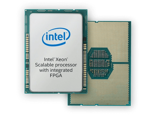
Back in 2018, Intel came up with a multi-chip module containing a Xeon Gold 6138P “Skylake-based” processor integrated with an Arria 10 GX field programmable gate array (FPGA). Here is what the chip package looks like, but this is just a CPU + FPGA combo on the same substrate, so this basically hinders the performance as well as the latency:
It remains to be seen when AMD will announce processors that take advantage of an FPGA unit. But it’s an interesting patent application and technology, nonetheless.
Stay tuned for more tech news!
Source: Hot Hardware.
Hello, my name is NICK Richardson. I’m an avid PC and tech fan since the good old days of RIVA TNT2, and 3DFX interactive “Voodoo” gaming cards. I love playing mostly First-person shooters, and I’m a die-hard fan of this FPS genre, since the good ‘old Doom and Wolfenstein days.
MUSIC has always been my passion/roots, but I started gaming “casually” when I was young on Nvidia’s GeForce3 series of cards. I’m by no means an avid or a hardcore gamer though, but I just love stuff related to the PC, Games, and technology in general. I’ve been involved with many indie Metal bands worldwide, and have helped them promote their albums in record labels. I’m a very broad-minded down to earth guy. MUSIC is my inner expression, and soul.
Contact: Email