
It appears that AMD has recently submitted a new patent to the US Patent and trademark Office/USPTO on December 31 2020, which outlines the company’s plan for its future GPU technology. This leak comes via Twitter user @davideneco25320 who spotted this entry.
The patent outlines a potential GPU chiplet design which AMD plans to implement. The patent’s filing date appears to be 06/28/2019, but AMD has filed and submitted similar MCM patents in the past as well.
According to AMD the conventional “monolithic” die designs are becoming increasingly expensive to manufacture, so the company plans to adopt a new GPU chiplet design. Due to the high latency between chiplets, an MCM approach was dropped in favor of a Monolithic design.
We can also expect massive yield gains from just shifting to an MCM based approach instead of a monolithic design. Despite having very poor yields, a single huge die was expensive to produce, and wastage was also an issue.
On Monolithic designs, the GPU programming model is often inefficient because the parallelism is difficult to distribute across multiple different working active groups and chiplets . It is also expensive design-wise to synchronize the memory contents of shared resources throughout the entire system, to provide a coherent view of the memory to applications.
Additionally, from a logical point of view, applications are written with the view that the system only has a single GPU. That is, even though a conventional GPU includes many GPU cores, applications are programmed as addressing a single device.
So, it has been historically challenging to bring chiplet design methodology to GPU architectures.
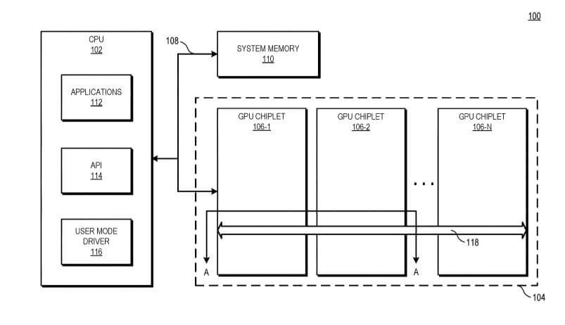
According to AMD such problems can be avoided by implementing a high bandwidth “passive crosslink”, which is basically an on-package interconnect. The first GPU chipset would be directly communicably coupled to the CPU, while each of the GPU chiplets in the array would then be coupled to the first GPU via a passive crosslink.
To improve system performance by using GPU chiplets while preserving the current programming model, AMD illustrated systems that will utilize high bandwidth passive crosslinks for coupling GPU chiplets.
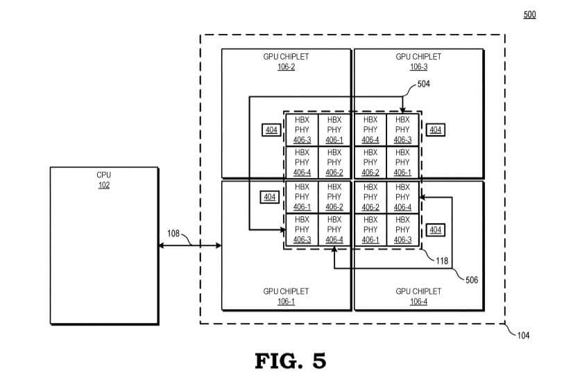
The said system includes a central processing unit (CPU) communicably coupled to a first graphics processing unit (GPU) chiplet of a GPU chiplet array. Basically the array includes the first GPU chiplet communicably coupled to the CPU via a bus, and a second GPU chiplet communicably coupled to the first GPU chiplet via a passive crosslink.
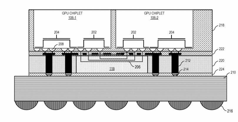
The passive crosslink is a passive interposer die dedicated for inter-chiplet communications. AMD plans to use a passive crosslink for communication between GPU chiplets, which are all on a single interposer.
This could mean that groups of GPU chiplets act like a System-on-a-Chip (SoC) which is divided into separate and different functional chips. This new chiplet design appears to suggest that each GPU chiplet will be a GPU in its own right and fully addressable by the operating system/OS as well.
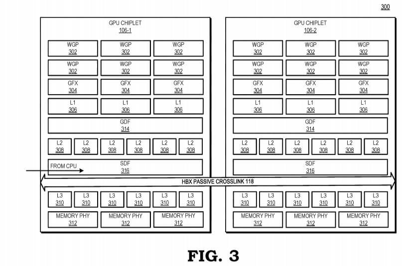
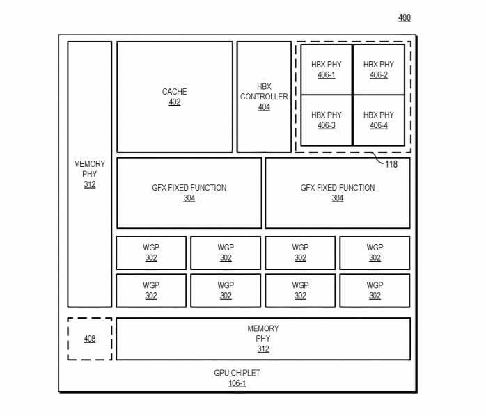
When it comes to the cache, currently various architectures already have at least one level of cache (e.g., L3 or other last level cache (LLC)) that is coherent across the entire conventional GPU die. But with this new patent design, the chiplet-based GPU architecture positions those physical resources (e.g., LLC) on different dies and communicably couples those physical resources such that the LLC level is unified and remains cache coherent across all GPU chiplets.
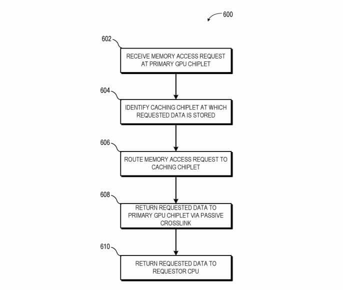
During operations, a memory address request from the CPU to the GPU is transmitted only to a single GPU chiplet, which then communicates with a high bandwidth passive crosslink to locate the requested data. From the CPU’s point of view, it appears to be addressing a single die, monolithic GPU.
This allows for use of a large-capacity, multi-chiplet GPU that appears as a single device to an application.
Such a design would see the cache being communicably coupled to other physical resources so that the cache stays unified and remains coherent across all GPU chiplets. Even though AMD has not officially confirmed it is working on such a GPU chiplet design, but there were rumors in the past that the future next-gen RDNA 3 architecture and its successors will be based on a multi-chip design.
AMD already has experience with a multi-chip design with the Ryzen CPU lineup and various APUs, and NVIDIA and Intel will both have their own GPU chiplet-style architectures in the coming years as well.
This is a block diagram illustrating a processing system employing high bandwidth passive crosslinks for coupling GPU chiplets in accordance with some embodiments.
This next block diagram illustrates a sectional view of GPU chiplets and passive crosslinks in accordance with some embodiments.
Block diagram illustrating a cache hierarchy of GPU chiplets coupled by a passive crosslink in accordance with some embodiments.
Block diagram illustrating a floor plan view of a GPU chiplet in accordance with some embodiments.
Block diagram illustrating a processing system utilizing a four-chiplet configuration in accordance with some embodiments.
This is a flow diagram illustrating a method of performing inter-chiplet communications in accordance with some embodiments.
It remains to see whether AMD indeed adopts this GPU chiplet design for its future RDNA architectures. For what it’s worth, Intel has already adopted a TILE-based design for its upcoming Xe-HP graphics cards, whereas NVIDIA is rumored to introduce its first MCM/multi-chip-module design with the next-gen Hopper architecture.
Stay tuned for more tech news!
Hello, my name is NICK Richardson. I’m an avid PC and tech fan since the good old days of RIVA TNT2, and 3DFX interactive “Voodoo” gaming cards. I love playing mostly First-person shooters, and I’m a die-hard fan of this FPS genre, since the good ‘old Doom and Wolfenstein days.
MUSIC has always been my passion/roots, but I started gaming “casually” when I was young on Nvidia’s GeForce3 series of cards. I’m by no means an avid or a hardcore gamer though, but I just love stuff related to the PC, Games, and technology in general. I’ve been involved with many indie Metal bands worldwide, and have helped them promote their albums in record labels. I’m a very broad-minded down to earth guy. MUSIC is my inner expression, and soul.
Contact: Email